The AFM5500M scanning probe microscope allows nanometer-scale observations of the three-dimensional morphology and mapping of the physical properties of sample surfaces to be carried out simultaneously. In addition, the system features wide-area flat scanners that enable highly linear scanning over a wide range up to 200 µm in the x and y directions, resulting in reduced image distortion. Moreover, by automating operations such as the installation and replacement of cantilevers, the adjustment of optical axes, and the configuration of measurement parameters, the AFM5500M significantly reduces the burden on operators. The system also features a combined AFM-SEM capability, which allows both AFM and scanning electron microscopy (SEM) measurements of the same region of a sample to be performed with ease.
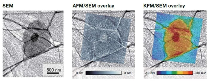
Example: Observation of the same region on a sample (graphene/SiO2) using both SEM and AFM.
Here, an AFM morphology image and a KFM potential image are superimposed on an SEM image.
See more
