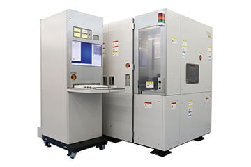
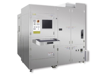
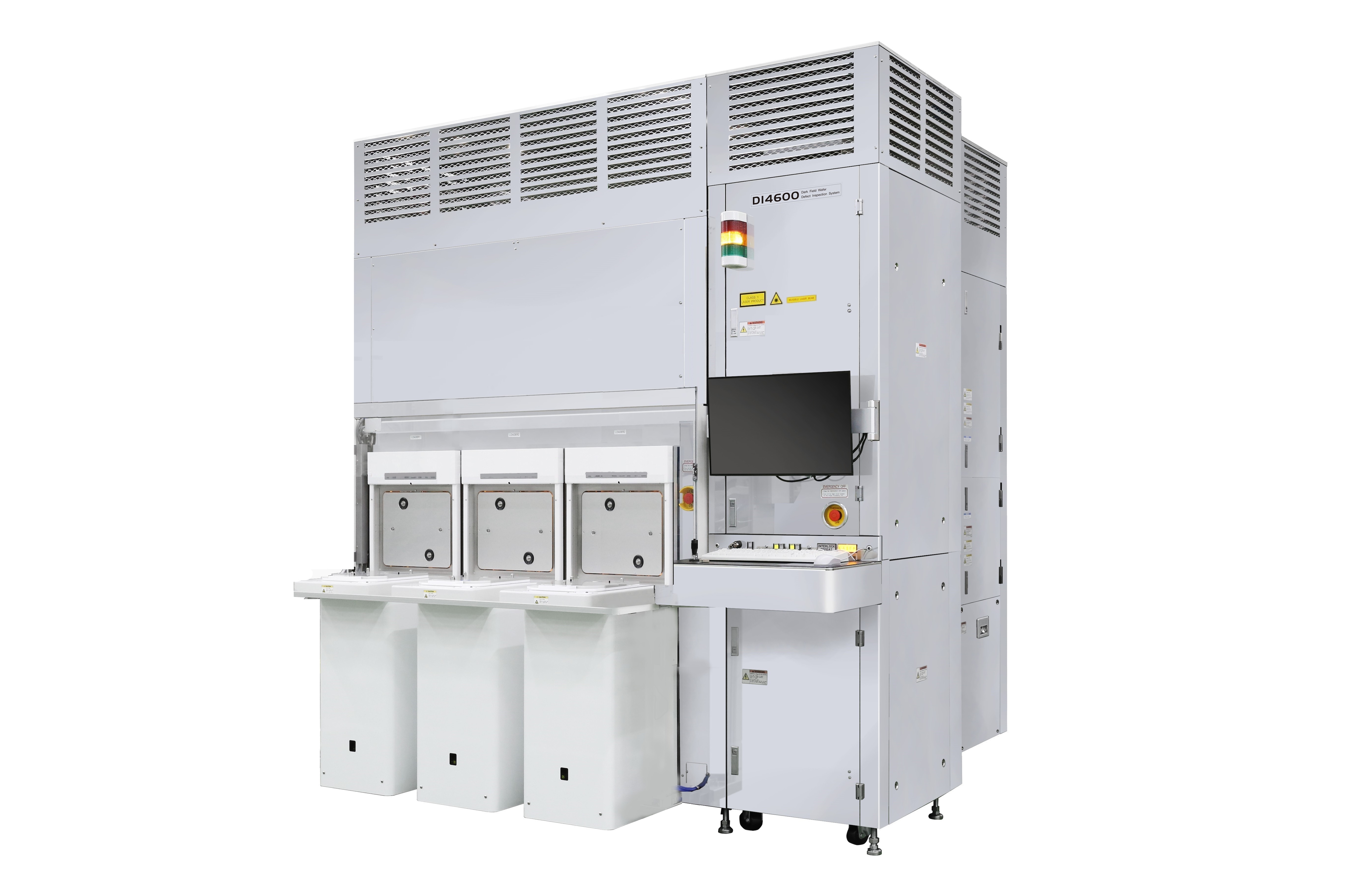
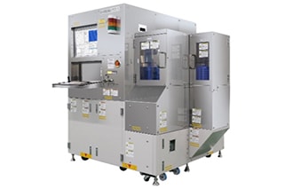
Dark Field Wafer Defect Inspection System DI2800
Contribution to defect detection and high-level process control of G&C device*1
DI2800 uses scattering-intensity simulation technology to optimize the illumination and detection optics, enabling highly sensitive inspection of patterned-wafer defects developed during the manufacturing process. It has a detection sensitivity of 0.1-μm standard particle size on mirrored wafers. This makes it possible to examine even the incredibly small, 0.3-mm square size chips used in semiconductor devices in the IoT and automotive fields, with optimization of the inspection sequence enabling a defect inspection speed of over forty 200-mm wafer sheets per hour.
*1
G&C device is an abbreviation for Green & Communication Device.
Specifically, electronic devices and electronic components manufactured
on φ100/125/150/200 mm wafers.
(Ex: SAW / BAW, MEMS and sensors, power and analog devices, etc.)
Features
- Defect detection by Hitachi’s original dark field inspection method
- Available for process monitor (Manufacturing process monitoring) and screening (Non-defective device selection)
- Support φ100 mm, φ150 mm, φ200 mm patterned/ non-patterned wafer
Specifications
| Inspection sensitivity | Detection of standard particle size 0.1 μm |
|---|---|
| Processing ability | At least 40 wafers per hour |