![]()
Tradition beauty of Minute
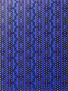
What of yours handle like? This is a new pattern this year. The true character of this picture is the arrangement of the tungsten plug after the CMP (Chemical and Mechanical Polishing) processing which is the important technology of realizing high-density multilayer wiring of a semiconductor device. This SEM image is produced by mixing a secondary electronic signal (Surface information) and backscattered electronic signal (Composition information). Don't you wear the tradition beauty which hi-technology produced, either?
At 58th photo contest hosted by the Japanese Society of Electron Microscopy in 2002.
Condition
Specimen: W plug wafer (CMP)
Instrument: Scanning Electron Microscope S-5200
Accelerating voltage: 3 kV
Observation mode: MIX mode (SE+BSE)
*All information related to these photographers is based on the information when the photo was taken.
*This work was presented at the "photo contest" hosted by the Japanese Society of Microscopy.
*Reproduction or republication without permission prohibited.
*"nanoart" is registered trademark of Hitachi High-Tech Corporation in Japan.
Products & Services
Related Information

Hitachi High-Tech Social Media