Sapporo nano Tower
© Yuka Nishimoto (Hitachi High-Tech Fielding corporation)
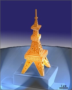
The micrograph shows a secondary electron(SE) image of the world's smallest tower prepared by a FIB (Focused Ion Beam) technique.
The specimen is extracted from a Si wafer by using a micro-sampling method and mounted on a needle stab of a specimen rotation holder. A towered shape is made by rotating the specimen. Although the FIB was initially developed for fixing and evaluation of semiconductor devices, such micromanipulation technologies have been made a further progress.
First Place (Field 1: Non-biology)
At the 16th International Microscopy Congress (IMC16), Micrograph Competition(2006).
Condition
Instrument (Fabrication): Focused Ion Beam System FB-2100
Accelerating voltage: 40 kV
Instrument (Observation): Ultra-high Resolution Scanning Electron Microscope S-5500
Accelerating voltage: 2 kV
*All information related to these photographers is based on the information when the photo was taken.
*This work was presented at the "photo contest" hosted by the Japanese Society of Microscopy.
*Reproduction or republication without permission prohibited.
*"nanoart" is registered trademark of Hitachi High-Tech Corporation in Japan.
Products & Services
Related Information

Hitachi High-Tech Social Media