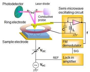
Scanning Non‐linear Dielectric Microscope(SNDM)
SNDM detects changes in electrostatic capacitance (∂C/∂V, ∂²2C/∂V², ∂³C/∂V³ ・・・) right underneath the probe as the resonance frequency of the semi-microwave oscillator approximately 1 GHZ by FM modulator, while applying an alternating current (VAC) between the probe and sample. Semiconductor carrier distribution and ferroelectric polarization domain can be observed. Recent research results show that SNDM observes low concentration level of 1013 atom/cm³.
* We have received guidance from Professor Cho at Tohoku University, the inventor of SNDM, to develop SNDM as a product.
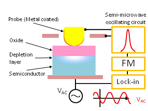
The slow-motion image shows changes in the depletion layer due to ac voltage when applying SNDM mode to a semiconductor material.
Si MOS transistor
Silicon solar cell
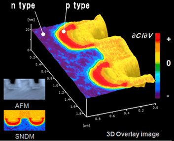
Advantages of Vaccum SNDM and C-V curve analysis p-n structure fabricated through ion implantation
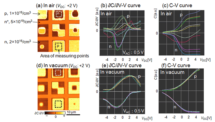
Vacuum SNDM eliminates effects of adsorbed water and enables more stable and high resolution ∂C/∂V-V curve and C-V curve measurements than in air.
Small n-type spot appeared on the vacuum SNDM image (d) was not observed in the SDNM image in air (a). ∂C/∂V-V curve and C-V curve (b, d) were separated in accordance with two different concentration levels of p-type and n-type in vacuum. In contrast, curves were unstable in air due to adsorbed water.
Jing-jiang Yu et al., "Environmental control scanning nonlinear dielectric microscopy measurements of p-n structures, epi-Si Wafers, and SiC crystal defects", ISTFA 2015: Conference Proceedings, 341-348, 2015.
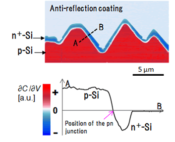
Vacuum SNDM measurements of SiC Power MOS FET and C-V analysis near pn junction
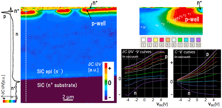
Carrier concentration mapping of SiC Power MOS FET in accordance with the device structure was obtained using vacuum SNMD. Throughout the 10 points of C-V curve measurements across p to n regions, the changes in the depletion layer is clearly obtained in response to concentration and domain. SNDM image and its signal cross section of Si solar battery clearly indicates the location of pn junction.
Polarization domain of single crystal potassium niobate (KNbO3)
The image shows the SNDM measurement result of potassium niobate single crystal in vertical polarization direction (d33 direction).
Products & Services
Hitachi High-Tech Social Media