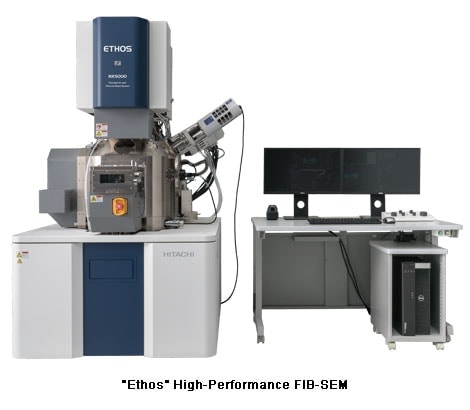
Hitachi High-Tech Corporation announced the development of an all-new high-performance "Ethos" Focused Ion Beam-Scanning Electron Microscope (FIB*1-SEM*2) that incorporates world-class Hitachi High-Tech core technologies in the form of a high-intensity cold-cathode field emission electron gun combined with a newly developed magnetic/electrostatic compound lens.
The Ethos FIB-SEM system incorporates a FIB column used in sample preparation along with the newest SEM concept for high-magnification observation, and is expected to become an essential tool for a wide range of fields such as semiconductors, nanotechnology, materials science, medicine, and biology for the study of sub-surface structures and the preparation of thin-film samples for Transmission Electron Microscopy (TEM*3) analysis. The Ethos FIB-SEM system enables the analysis of microscopic surface structure and topography at the micron scale, especially in the fields of high-performance devices and nanomaterials, where miniaturization has been advancing recently. The Ethos system is designed to play an important role in the preparation of uniformly thin, high-grade TEM samples for observation and analysis of fine structure at atomic levels, as well as for defect analysis and evaluation.
The Ethos FIB-SEM system enables high-resolution imaging at low acceleration voltages, and by combining with ACE*4 technologies (technologies that suppress curtaining effects or striations*5 during cross-section sample preparation), which enable high-grade TEM sample preparation, the Ethos FIB-SEM system is capable of preparing high-grade and high-quality TEM samples uniformly in its triple-beam configuration.
The Ethos FIB-SEM system is designed with an innovative large-volume sample chamber equipped with ports for Energy Dispersive X-ray Spectrometer (EDS*6) and Electron Backscatter Diffraction (EBSD*7), along with a multitude of additional analytical detection configurations possible with optimum detector positioning. The sample chamber is designed for users who are prepared for customization and upgradeability in the future. Samples can be processed and observed from all angles with a large 155-mm X-Y stage. Design considerations for the modern scientists in every field delivers Ethos for looking at not only the latest semiconductors, but also everything from biological samples to magnetic materials such as steel.
*Optional
| SEM optical system | |
|---|---|
| Electron source | Cold-cathode field emission type |
| Accelerating voltage | 0.1-30 kV |
| Resolution | 1.5 nm (1 kV), 0.7 nm (15 kV) |
| FIB optical system | |
| Accelerating voltage | 0.5-30 kV |
| Maximum beam current | 100 nA |
| Resolution | 4.0 nm (30 kV) |
| Stage | |
| Movable range | X: 0-155 mm, Y: 0-155 mm, Z: 0-16.5 mm, T: -10-59°, R: 360° *Stroke may be restricted by the sample holder. |
| Sample size | 150 mm diameter max. |
See more
