
Tae Woong Kim*
Ph.D.
Assistant Professor
Department of Energy Material Science
College of Science and Technology
Konkuk University
*corresponding author

Satoshi Uchida
Ph.D. (Engineering)
Project Professor
Research Center for Advanced Science and
Technology
The University of Tokyo
Photo-voltaic cells (PVCs) made from organo-halide-perovskites are next-generation PVC devices that boast dramatically reduced manufacturing costs and are a subject of eager anticipation from all corners of the globe. As of January 2019, these devices have been officially recorded as offering a conversion efficiency of 25.2% on the NREL chart1)—a figure which outclasses that of CIGS (23.4%) and polycrystalline silicon (22.3%) and represents stunning performance improvements over the past few years. Indeed, it is difficult to remember that the performance of organic PVCs seemed permanently doomed to lag far behind that of inorganic cells. However, while there have been an enormous number of reports of research studies targeting the challenge of increased efficiency, analysis of the crucial perovskite material comprising the PVC—including ultra-miniature observations of its nanoscale crystal structure—involves difficult technical challenges and has not been extensively pursued to date despite the high level of interest. In this paper we report that the use of focused-ion-beam (FIB) techniques for sample processing, combined with transmission electron microscopy (TEM), offers an extremely powerful approach to the observation of organo-halide perovskite PVC cells2, 3).
Discussions of experimental observation of perovskite PVCs are invariably accompanied by anxiety regarding the risk of sample damage induced by electron-beam irradiation due to physical vulnerabilities in the sample. However, if one simply investigates and addresses each individual instance of damage, it is not particularly difficult to determine whether an observed image accurately depicts the actual sample or is corrupted by the presence of sample damage. I am sure readers already know about this, but incidents of electron-beam damage and the associated consequences may broadly be divided into the following three categories5):
Figure 1 depicts the observed states of an actual perovskite PVC imaged by a Hitachi HF-3300 field-emission transmission electron microscope (FE-TEM). In the image captured 10 seconds after the start of the observation, the electron-beam diffraction image appears unchanged; however, after 4 minutes the electron-beam diffraction image has evolved from a spot to a hollow ring, and there are indications of the emergence of non-crystalline matter. We attribute both of these effects to radiolysis or knock-on.
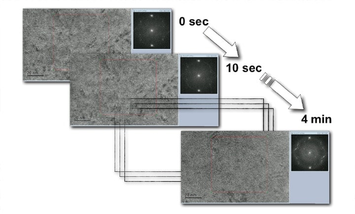
Fig. 1 Temporal evolution of observed images showing the effect of damage to a CH3NH3PbI3 perovskite due to radiolysis and knock-on phenomena
Thermal damage is also a cause for concern. Figure 2 shows plots of typical relationships between beam currents and increases in sample temperatures4). We have extrapolated thermal conductivity values5) for the material we observe, CH3NH3PbI3 (MAPbI3). From the points at which the graphs intersect, we obtain the theoretical prediction that this material will increase in temperature at a rate of approximately 1°C/sec. Because MAPbI3 undergoes a phase transition6) (from tetragonal to cubic) at temperature near 55°C, if we consider an observation in which the sample starts at room temperature of 25°C, we have a temperature-increase budget of just ΔT=30K before the onset of the phase transition, and we must complete our observation within 30 seconds to avoid raising discussion about issues other than sample damages.
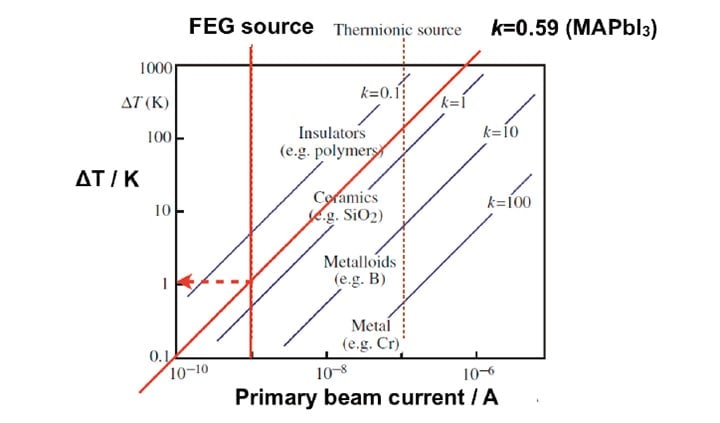
Fig. 2 Prediction of sample heating for observation of a CH3NH3PbI3 perovskite
In our actual experiments, we continued the MAPbI3 sample observation holding the field of view fixed; this allowed us to observe the emergence of black particles, exhibiting crystalline growth, from the flat image (Figure 3). EDX composition analysis confirmed that these were PbI2 particles remaining after the escape of methylamine molecules (CH3NH3+), which are organic molecules.
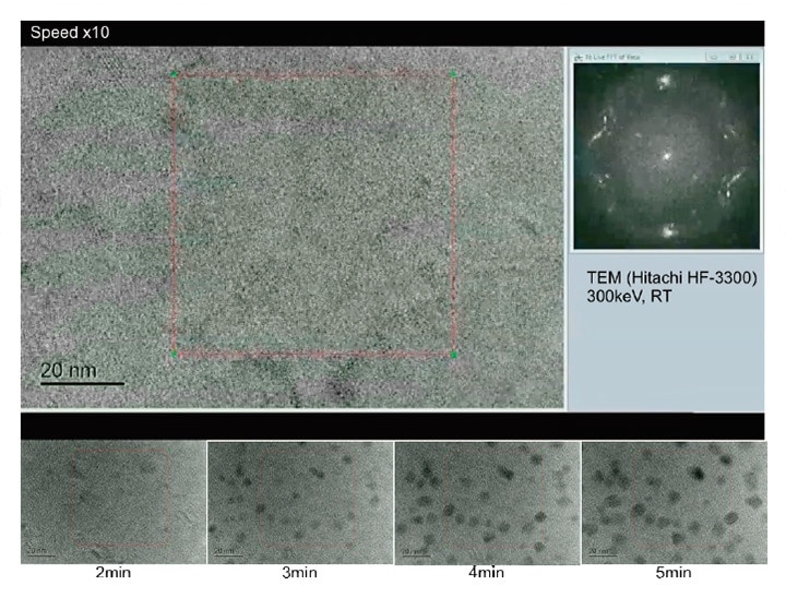
Fig. 3 Example of the temporal evolution of a CH3NH3PbI3 perovskite sample under observation
In view of the various aforementioned limitations imposed by electron-beam damage, we adopted an experimental protocol for observation of perovskite PVCs in which we inspected the sample as quickly as possible, adjusted the focus and noted its setting, then (typically within 5 seconds) moved on to the next sample area. In addition, the risk of damage due to the use of FIB techniques to fragmentize the sample must be held to a minimum by reducing the accelerating voltage and otherwise making judicious choices for the configuration of beam settings. To prove that the TEM images we present below are not artifacts due to FIB damage, we compared observations of our actual sample against observations of a sample of powder formed by filing a glass substrate and confirmed that there was no difference in the corresponding features.
Figure 4 is a high-resolution TEM observation of a thin-film sample of CH3NH3PbI3, the well-known perovskite material used in PVCs. In contrast to our expectations, we observe a coexistence of tetragonal and cubic phases depending on the sample region observed. The observation of the cubic phase—a high-temperature phase that should not exist at room temperature—came as a major surprise; to explain it, we note that this PVC is an extremely thin film of thickness just 300–500 nm, and we surmise that, in the process of cooling from a heated state to room temperature during our fabrication procedure, some cubic-phase regions of the sample were quenched and remained in place thereafter, as shown in Figure 5.
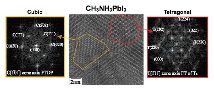
Fig. 4 Coexistence of tetragonal and cubic phases at room temperature in a thin film of CH3NH3PbI3 perovskite (Hitachi HF-3300)
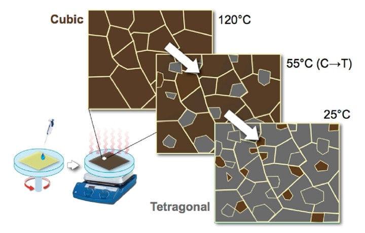
Fig. 5 Predictive model to explain the coexistence of tetragonal and cubic phases in CH3NH3PbI3 perovskite thin film
Further observations revealed the presence of occasional superlattice structures. Figure 6 shows (a) a TEM image, (b) an electron-beam diffraction image, and (c) a Fourier-transform image calculated from (a) and (b). The measurements show that the distance between planes of the lattice structure is 10.989Å. Such large values of d do not exist in conventional CH3NH3PbI3 perovskites, but the feature is an unmistakable signature of the perovskite structure. Although the conclusions derived from our TEM observations ultimately yield only distance-related information—and thus inferences are necessarily somewhat speculative—we suspect that the superlattice structure was formed by a tetragonal-cubic-tetragonal sandwich that together constitutes one long period. Regarding the locations at which superlattice structure is present, we observe it in intermediate regions connecting tetragonal to cubic domains, and at regions of the underlying substrate connecting TiO2 phases to perovskite phases; in both cases the superlattice emerges naturally to allow relaxation of mild lattice strain (Figure 7).
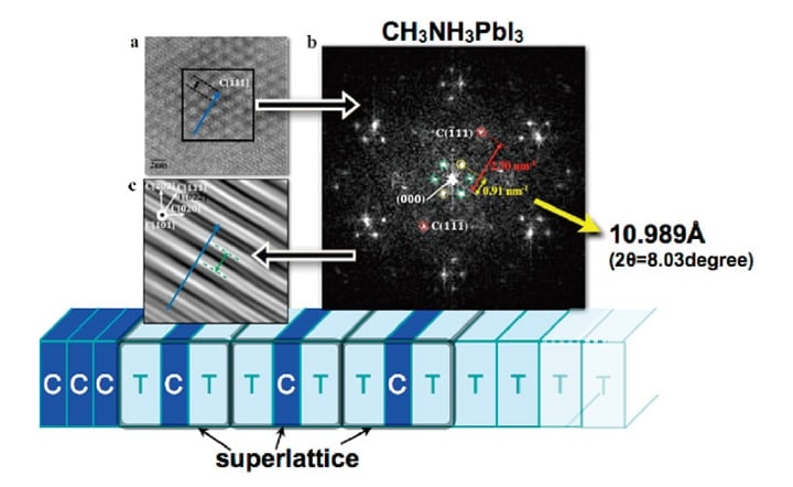
Fig. 6 Observation of superlattice structure in a thin film of CH3NH3PbI3 perovskite. (a) TEM image. (b) EDS image. (c) Fourier-transform image.
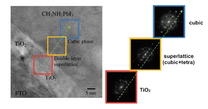
Fig. 7 TEM image of superlattice structure observed in a thin film of CH3NH3PbI3 perovskite
For reference, as a comparison experiment we measured a sample cut via FIB from a 1 mm square single crystal and observed no cubic phases or superlattice structures. Although we cannot rigorously prove that such features are in fact entirely absent, we accumulate information on the sample as a whole via TEM observations at low magnification and confirm that in depth (dark/light shading) analysis in 4 directions with different diffraction angles, all the signal-intensity waveforms are all symmetric with respect to the center. The absence of the biased peaks and shoulders observed in the presence of cubic-phase coexistence indicate a uniform tetragonal phase (Figures 8, 9).
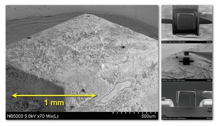
Fig. 8 Procedure for FIB processing of single-crystal CH3NH3PbI3 perovskite sample
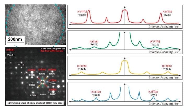
Fig. 9 TEM image, EDS image, and comparison of signal intensities in the depth direction for single-crystal CH3NH3PbI3 sample
Perovskite PVCs are an emerging technology for which high efficiencies have been recorded in laboratory settings, but for which many hurdles—particularly regarding durability—remain to be overcome to achieve practical utility. Of course, the very existence of these challenges serves to whet the problem-solving appetite, and going forward we anticipate large numbers of researchers joining the field to ensure an intensely competitive R&D climate. At the same time, our understanding of the basic operating mechanisms of these devices remains inadequate, and electron-microscope observation is an essential tool for understanding device structure. In particular, the presence of superlattice structures and the other unusual nanoscale features discussed above are intimately related to photoelectric conversion properties, and basic insights of this sort may be of enormous practical advantage for achieving yet further increases in efficiency.
In conclusion, we showed in this work that the combination of FIB-based sample fragmentation with TEM observation is an extremely powerful tool for observation of fine-grained structure.
Acknowledgements
In performing the measurements reported here, we received comprehensive and thorough support from the staff of Hitachi High-Tech Corporation, to whom we express our deepest gratitude.
References
See more
