Masako Nishimura*1、Kaori Ichikawa*2、and Masahiko Ajima*1
Fig.1 The Hitachi TM3030Plus tabletop microscope.
The TM3030Plus tabletop microscope1-4) are low-vacuum scanning electron microscopes (SEMs) that allow easy observation and analysis—without specimen preparation—of samples including even non-conductive materials or materials containing water or oil. These instruments have found widespread application at all stages of the product-design process—from research and development to quality control—and across a wide range of industrial sectors including the materials, electrical and electronics, foodstuffs, and biotechnology industries. The newly developed TM3030Plus model (Fig. 1) adds the additional advantage of a low-vacuum secondary electron detector5)—of the same type installed on higher-level SEM models—allowing the new possibility of secondary electron observations in low-vacuum environments. In this report, we present a number of sample applications that illustrate the expanded applicability of the TM3030Plus while emphasizing the ease-of-use of this product line.
In conventional high-vacuum SEMs, the usual secondary electrons are used as the detected signal, yielding images that reflect the roughness morphology of the sample surface. However, because the energies of the secondary electrons are extremely small—10 eV or less—in low-vacuum environments they easily lose energy through collisions with residual gas molecules and fail to arrive at the standard secondary electron detectors used in high-vacuum environments. For this reason, in low-vacuum observations, the backscattered electrons (which have roughly the same energy as the incident electrons) are detected as the signal used to form an image. The efficiency with which backscattered electrons are emitted increases as the mean atomic number of the sample increases, yielding brighter images; for this reason, the backscattered electron image provides contrast reflecting differences in rough composition within the sample.
In contrast, the TM3030Plus—as shown in Figure 2—is equipped with the same low-vacuum secondary electron detector installed on higher-level SEM models, allowing the observation of secondary electrons. Secondary electrons emitted from the sample are accelerated by the electric field of bias electrodes positioned near the detector; the accelerated electrons collide with residual gas molecules, dissociating those molecules into an electron and a positive ion and emitting an excitation photon. Due to acceleration, this dissociation process repeats many times, yielding an exponential increase in the numbers of positive ions and electrons and the excitation photons emitted in conjunction. The low-vacuum secondary electron detector detects these excitation photons to produce images; because the excitation photons contain information on the secondary electrons, one obtains images even under low-vacuum conditions that reflect the roughness morphology of sample surfaces in ways similar to the results of secondary electron images under high-vacuum conditions.
In a sample observation involving a diamond bit with backscattered electron and secondary electron images obtained with the same field of view, the backscattered electron image stores composition information by reflecting the mean atomic number of the sample, while the secondary electron image reflects the roughness morphology of the sample surface.
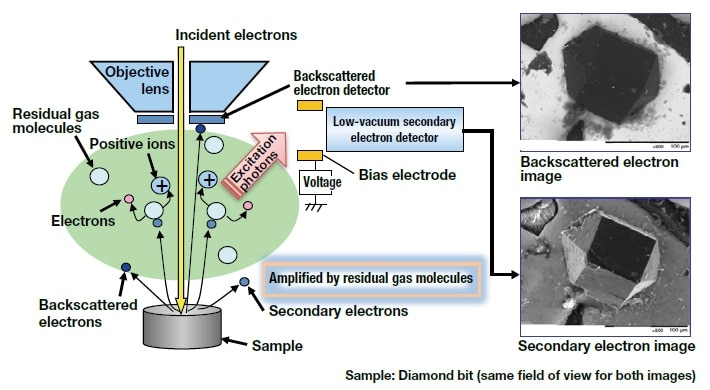
Fig. 2 Signal detection and imaging in low-vacuum observations.
By performing mixed image observations in which backscattered electron images are mixed with secondary electron images, we obtain simultaneous observations of the composition and the roughness morphology of the surface.
Switching between backscattered electron, secondary electron, and mixed images is as easy as clicking a single button on a GUI. Figure 3 shows backscattered electron and secondary electron images (obtained with the same field of view) of a ruptured ceramic surface, together with the mixed image. From the backscattered electron image, we obtain clear information on the composition of the sample—specifically, on the distribution of zirconia (bright regions) among alumina (dark regions)—while in the secondary electron image, we see the roughness morphology of the ruptured surface. From the mixed image, we are able to obtain both types of information simultaneously.
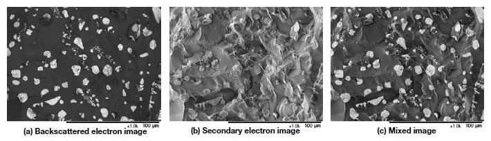
Fig.3 An example involving observations of a ruptured ceramic surface.
Accelerating voltage: Surface mode (5 kV)/ Observation mode: Standard mode (30 Pa)/ Magnification: 1,000×
Because the Energy Dispersive X-ray Spectrometer (EDS) included in the TM3030Plus is a large detection area (30 mm2) silicon drift detector (SDD), it allows rapid and highly efficient qualitative analysis and element mapping. Figure 4 shows mapping results for the ruptured surface of a varistor (a type of electronic component). Using EDS analysis, we are able to obtain the distribution of various elements in just a matter of minutes.
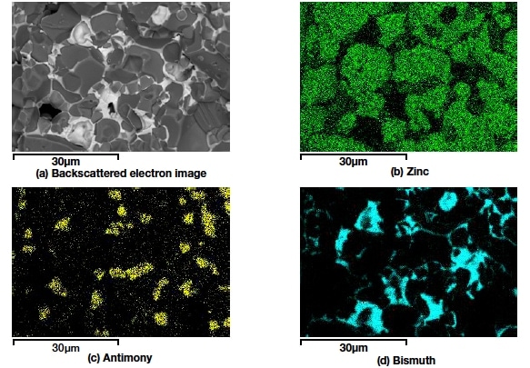
Fig.4 Results of EDS analysis of a ruptured varistor surface.
Accelerating voltage: Analytical mode (15 kV)/ Observation mode: Charge-reduction mode (50 Pa)/ Magnification: 3,000×
Figure 5 shows backscattered electron and secondary electron images, obtained with the same field of view and with no metallic coating, of high-quality paper on which letters have been imprinted by a laser printer. The right half of the image corresponds to a printed region of the page. In the backscattered electron image, the calcium carbonate present in high-quality paper is clearly indicated by regions of bright contrast showing changes in material composition. Meanwhile, from the secondary electron image, we glean three-dimensional information on the roughness of the fibers in the high-quality paper and on the nature of the adhesion of toner to paper (arrows).
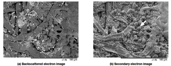
Fig.5 A sample observation of high-quality paper on which letters have been imprinted by a laser printer.
Accelerating voltage: Surface mode (5 kV)/ Observation mode: Charge reduction mode (50 Pa)/ Magnification: 1,000×
Figure 6 shows images—taken as is, with no pre-processing, using the same field of view—of a thin coating of toothpaste on the sample stage. In the backscattered electron image, we observe high-contrast regions corresponding to the polishing agents present in the toothpaste; from the secondary electron image, we glean information about the roughness morphology of the coating. From the mixed image, we simultaneously obtain information on material composition and roughness morphology.
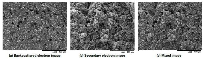
Fig.6 A sample observation of toothpaste.
Accelerating voltage: Surface mode (5 kV)/ Observation mode: Charge reduction mode (50 Pa)/ Magnification: 600×
Figure 7 shows images, obtained with no metal coating using the same field of view, of eye shadow. Images (a) and (b) are backscattered electron and secondary electron images obtained at an accelerating voltage of 15 kV, while images (c) and (d) are backscattered electron and secondary electron images obtained at an accelerating voltage of 5 kV. Comparing images obtained at the same accelerating voltage, we see that backscattered electron images yield information on material composition, while secondary electron images yield clear information on the roughness morphology of the sample surface. Comparing images at accelerating voltages of 15 kV and 5 kV, we see that, at 5 kV, the incident electrons don't penetrate deeply into the sample, and thus backscattered electron image (c) yields more detailed information than image (a) on fine-grained variations in the material composition of the sample surface, while secondary electron image (d) yields more detailed information than image (b) on the three-dimensional structure of the sample surface. Thus we see that a wide range of information may be obtained by optimizing the signal chosen and the accelerating voltage for specific samples and analysis.

Fig.7 Observation of eye shadow.
Observation mode: Charge reduction mode (50 Pa)/ Magnification: 2,000×
Figure 8 shows a sample secondary electron image obtained from biological samples pre-processed for high-vacuum SEM observation. (a) is a kidney glomus subject to a preprocessing sequence consisting of fixing-water removal-drying-metal coating, while (b) is a cross section of a metal-coated scale from a butterfly wing. The metal coating improves the emission efficiency of secondary electrons, allowing sharp images with strong signals similar to those typically obtained under high-vacuum conditions to be obtained even in low-vacuum observations.
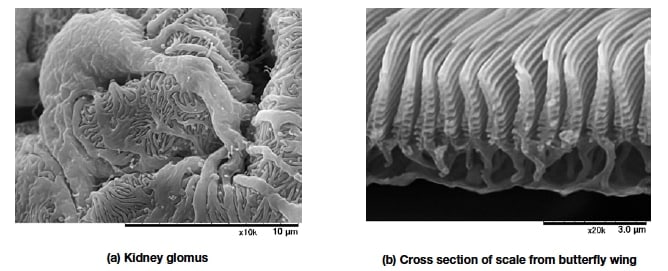
Fig.8 Sample observations of biological samples.
Accelerating voltage: Standard mode (15 kV)/ Observation mode: Standard mode (30 Pa)/ Magnification: (a) 10,000× (b) 20,000×
By incorporating a low-vacuum secondary electron detector, the TM3030Plus allows backscattered electron images to be augmented by new secondary electron images—even under low-vacuum conditions—as well as mixed images. With no need for sample pre-processing, one rapidly obtains information on both the material composition and roughness morphology of the sample surface, promising a wide range of applications involving multifaceted characterization and analysis studies across a wide range of fields of research.
References
Authors
See more
