―Equipped with Extra-Large Chamber and Heavy-Sample Stage―
Masanari Furiki
For the dual objectives of (a) accommodating samples of large sizes and heavy weights, and (b) improving ease of operation by automating the measurement process and enabling wide-area camera navigation, we have recently added two new models to Hitachi’s lineup of scanning electron microscopes (SEMs): the medium specimen chamber model SU3800 and the extra-large specimen chamber model SU3900.
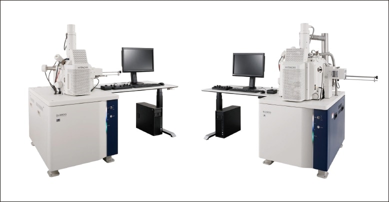
Fig. 1 Hitachi’s new scanning electron microscopes SU3800 (left) and SU3900 (right).
SEMs are used in nanotechnology, biotechnology, and many other industrial sectors for a wide range of observational and analytical purposes, from visualizing the fine-grained structure of substances to identifying their composition. As the range of SEM applications broadens to encompass new fields and new objectives, the need to observe samples of large sizes and heavy weights—including automotive components and industrial materials such as iron and steel—has been increasingly problematic due to limitations posed by SEM sample stages on the sizes and weights of samples, which have often required samples to be cut into smaller pieces or otherwise processed before mounting for observation.
In addition, recent years have witnessed a growing need to control the fine-grained structure of various types of materials in pursuit of enhanced functionality and improved performance, whereupon the range of practical uses for SEM technology has broadened beyond conventional R&D applications to encompass areas such as quality assurance and manufacturing process controls—fields in which SEMs are used with increasing frequency. These developments have created a need for improved ease of operation to reduce the practical burden shouldered by SEM operators.
The SU3800 and SU3900 are designed both to facilitate observation of large, heavy samples and to offer improved ease of operation. In particular, the SU3900, as Hitachi High-Tech’s extra-large chamber model, is equipped with our largest-class sample stage—of diameter 300 mm(*1) and maximum sample weight 5 kg (2.5 times heavier than previous-generation models(*2))—allowing observation of large samples with no need for cutting or other sample processing. Moreover, the measurement process following sample mounting—from electron-beam irradiation to image adjustment—has been automated to allow acquisition of SEM images immediately after the start of observations, enabling a speedy observational workflow.
Also, the task of searching for a target field of view—for which conventional instruments use a single color image captured by optical camera—is streamlined by our camera navigation technology, in which the sample stage is rotated to capture multiple partial images of the sample, which are then stitched together into a composite whole image to facilitate field-of-view searching for wide-area observation of large samples.
Both new instruments offer an increase in maximum mountable sample size. The SU3800 is equipped with a specimen chamber of diameter 200 mm, accommodating samples of height up to 80 mm and weight up to 2 kg. The SU3900, as Hitachi High-Tech’s extra-large chamber model, is equipped with our largest-class specimen chamber, of diameter 300 mm, accommodating samples of height up to 130 mm and weight up to 5 kg, 2.5 times heavier than previous-generation models(*2).
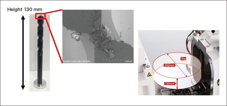
Fig. 2 An example of an observation involving a large sample (height 130 mm)
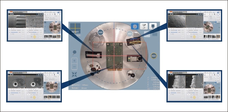
Fig. 3 Using wide-area SEM MAP to select the field of view
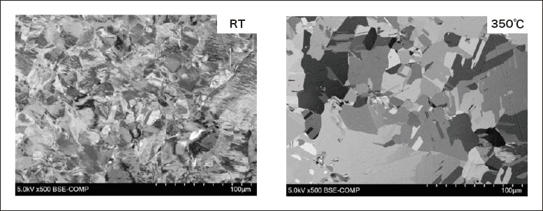
Fig. 4 Observation of a copper slab using the heating stage. Left: room temperature. Right: 350°C.
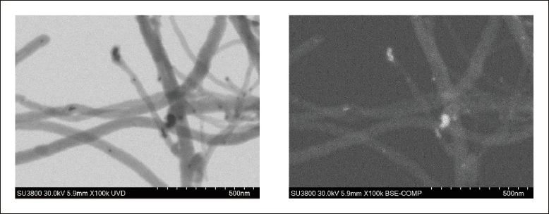
Fig. 5 Observation of carbon nanotubes using the new STEM holder. Left: Bright-field STEM image. Right: Backscattered-electron image.
| Item | SU3800 | SU3900 |
|---|---|---|
| Secondary-electron image resolution | 3.0 nm (Accelerating voltage 30 kV, high-vacuum mode) 15.0 nm (Accelerating voltage 1 kV, high-vacuum mode) |
|
| Backscattered-electron image resolution | 4.0 nm (Accelerating voltage 30 kV, low-vacuum mode) | |
| Accelerating voltage | 0.3-30 kV | |
| Magnification | ×5-×300,000 (photograph magnification), ×7-×800,000 (true display magnification) |
|
| Sample stage | X: 0-100 mm, Y: 0-50 mm, Z: 5-65 mm, T: −20°-90°, R: 360° |
X: 0-150 mm, Y: 0-150 mm, Z: 5-85 mm, T: −20°-90°, R: 360° |
| Maximum mountable sample size | 200 mm diameter | 300 mm diameter |
| Maximum observable range | 130 mm diameter (used with R) | 200 mm diameter (used with R) |
| Maximum sample thickness | 80 mm (WD=10 mm) | 130 mm (WD=10 mm) |
| Maximum sample weight | 2 kg | 5 kg (without T/R) |
About the author
Masanari Furiki
Metrology and Analysis Systems Division
Nano-Technology Solution Business Group
Hitachi High-Tech Corporation
See more
