Junji Kuwahara
The complementary fields of surface processing technology and surface-morphology / roughness metrology exist in a symbiotic relationship that is often likened to that among the wheels of a car: by perpetually incorporating innovative new architectural technologies, the two fields evolve on a daily basis—in a quest to accommodate the needs of the industrial world—while simultaneously striving to maintain a healthy balance.
At first, the innovation of non-contact techniques for surface-morphology and roughness metrology—based on the use of laser displacement gauges enabled by laser optics technology, a field that has blossomed rapidly in recent years—spurred an evolution away from the contact-probe metrology methods that had been used in the past, furnishing an opportunity to address a number of problems that had long afflicted contact-probe techniques. Later, the combination of laser displacement gauges with electrically-actuated XY stages birthed the possibility of plotting displacement-gauge height information as a function of X and Y coordinates, effecting a transition from an earlier era of line measurements into the modern realm of area measurements—and, in the process, addressing four practical difficulties that had complicated measurements for years, namely.
The subsequent advent of laser scanning metrology (LSM), in which the optical chassis of a microscope is used to effect in-plane scanning while acquiring detailed surface information, spurred yet another dramatic expansion of the range of possibilities for characterizing surface morphology and roughness, transcending the limitations of linemeasurement methods to usher in a new era of 3D surface-morphology metrology via non-contact area measurements.
In the early days of this new era of practical non-contact area measurement, measurement instruments and processing tools with precision on the order of microns sufficed to satisfy most industrial needs, and methods of LSM that matched these needs came into widespread use throughout the industrial world. However, in recent years the growing precision of surface-treatment methods has placed increasingly stringent demands on the accuracy of measurement and processing techniques, which are now routinely required to achieve tolerances on the order of nanometers; the metrological performance of LSM techniques has failed to keep pace with these precision requirements, and this has created new problems for the field. At the same time, a new metrological requirement—the capability for measurement of nanometer-scale surface undulations in wider sample areas—has become prominent, and the industrial world has begun gradually to shift from conventional LSM methods to a new generation of instruments based on coherence scanning interferometry (CSI) techniques, which offer promising technological solutions for some of industry’s new requirements, including
To give just one example, the fields of R&D and manufacturing process technology for products such as functional films, flat-panel displays, and various types of devices have come to require not only surface-roughness measurements over small in-plane areas of sizes on the order of 100 microns, but also measurements of roughness and undulations—with nanometer precision in the vertical direction—over wide in-plane areas of sizes of 1 millimeter or above. The difficulty of achieving satisfactory resolution and measurement reproducibility with LSM techniques has spurred the development of a new generation of CSI-based instruments capable of characterizing surface morphology and
roughness from multiple angles.
Thus we see that measurement instruments, driven by the need to keep pace with major changes in the processing techniques and industrial needs of each era, have exhibited continual evolution, proceeding from line to area measurements and from LSM to CSI techniques. In this report, we present the CSI-based Nano 3D Optical Interferometry System VS1800, discussing both the measurement technology underlying the instrument and a variety of application case studies.
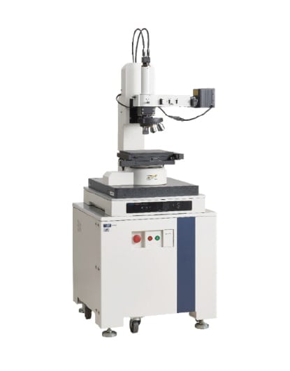
Fig. 1 The Nano 3D Optical Interferometry System VS1800
The Nano 3D Optical Interferometry System VS1800 is a system for 3D surface-morphology and roughness measurements that includes a microscope chassis equipped with a white-light source, double beam interference objective lenses—including Mirau and Michelson lenses—actuated in the vertical direction by motors and PZT elements, and a camera to capture interference-fringes.
To begin, Figure 2 illustrates the metrological principles of the instrument. The camera—a light-receiving element corresponding to the extent of the in-plane measurement field of view—detects the presence of interference-fringes created by a double beam interference objective lens and captures variations in these fringes due to vertical scanning of the objective lens, actuated by the vertical motions of motors and PZT elements; changes in interferometric intensity at each camera pixel are observed for the entire in-plane region of a measurement, and this data is processed by an analytical algorithm to yield high-precision measurements of 3D surface morphology and roughness.
The instrument offers a variety of measurement modes: Phase mode, which focuses on phase shifts, Wave mode, which acquires interference-fringe data for the entire field of view by scanning in the Z-axis direction and connecting the successive interference-fringes that result; Focus mode, in which the height at a given point is determined from the Z-axis position at which the interference intensity is greatest; and Film thickness-measurement mode, used for multilayer film thickness measurements.
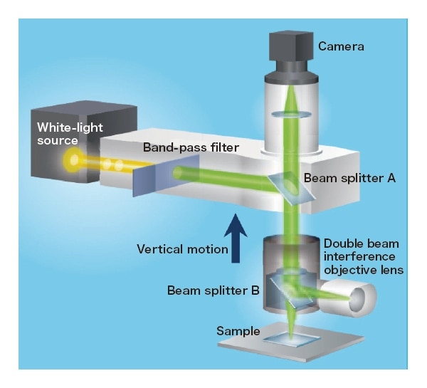
Fig. 2 Schematic diagram of the instrument
Next, Table 1 lists the key features of the Nano 3D Optical Interferometry System VS1800 together with comparisons to various other methods of measurement, including LSM and contact-probe metrology.
The Nano 3D Optical Interferometry System VS1800 is an instrument allowing non-contact area measurements. This eliminates two problems of contact-probe techniques: sample damage due to contact pressure and dependence of measurement results on data-acquisition direction. In addition, compared to LSM methods—which also perform area measurements—the VS1800 not only offers higher vertical resolution and height repeatability, extremely short measurement times due to vertical scanning actuated by motors and PZT elements alone (on the order of seconds), but also does not base its measurements on variations of the focal-point position in the vertical direction. The latter eliminates a common problem with LSM techniques, which is the dependence of the vertical resolution on the in-plane measurement area (that is, on the magnification factor of the lens) due to the differences in the focal-point depth of lenses with different magnifications.
Table 1: Comparison of the VS1800 to LSM and contact-probe techniques
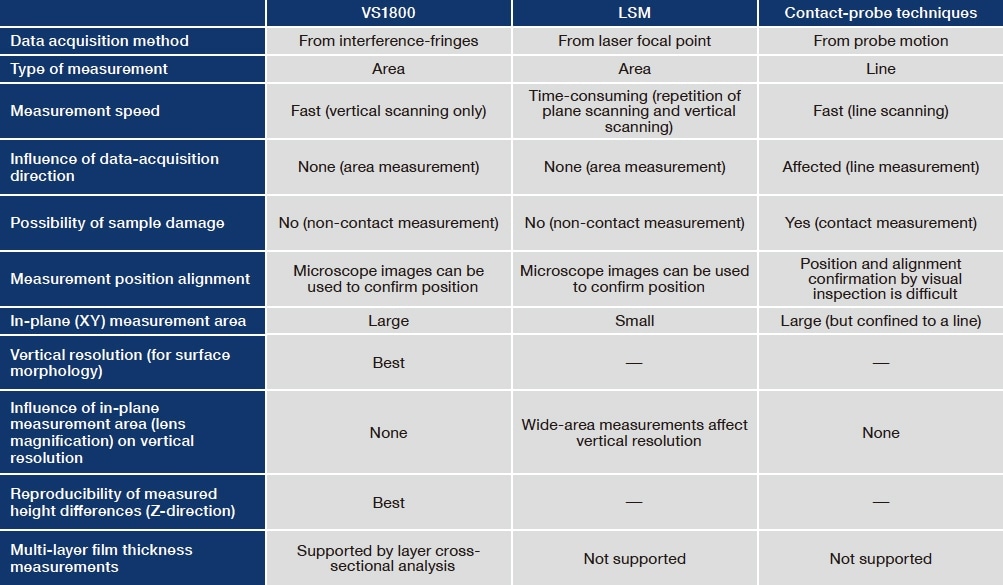
Note: “Best” indicates superiority among the three methods considered here.
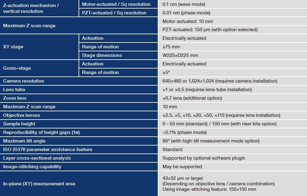
Finally, Table 2 lists the specifications of the Nano 3D Optical Interferometry System VS1800 Type 3. The VS1800 offers three sets of base specifications: Type 1, in which both the in-plane (XY) stage and the sample-tilt gonio-stage are controlled manually; Type 2, in which the in-plane stage is electrically actuated and the gonio-stage is controlled manually; and Type 3, in which both the in-plane stage and the gonio-stage are electrically actuated. The choice of Type 2 or Type 3 instruments further expands the sample area available for measurements by offering the ability to stitch together images, a feature provided together with the electrically-actuated in-plane stage.
These base specifications may be augmented by selecting additional options—including lens-camera combinations, the presence or absence of a PZT element for Z-axis actuation, riser kits to accommodate large samples, and various additional analytical features—that lend the instrument a flexible design and the potential to customize it to span a wide spectrum of metrological needs. Particularly deserving of mention is, high-tilt measurement mode, which offers measurements at sample angles up to 86° (when using the 400-micron SUS sphere); this facilitates measurement of steep slopes—whose difficulty in conventional CSI systems is considered a shortcoming of CSI techniques—with no sacrifice in performance compared to LSM techniques, greatly expanding the range of possible observation samples.
Other noteworthy features of the instrument—including ISO 25178 parameter assistance and layer cross-sectional analysis—are discussed in the following section in conjunction with application case studies.
Table 2: Specifications of the Nano 3D Optical Interferometry System VS1800 Type 3
The new technology of room-temperature bonding is useful for bonding wafers with different thermal expansion coefficients at room temperature without the use of adhesives, and has become an important tool for fabricating nextgeneration high-performance devices such as power devices and optical devices. The strength of junctions formed by room-temperature bonding is greater when the surfaces of the joined samples are smooth, and numerical control of surface roughness via ultra-smoothing treatments such as CMP polishing or atomic diffusion has come to be understood as a key tool for controlling the strength of junctions—or the possibility of forming any junction at all. The surface roughness of wafers used in room-temperature bonding has conventionally been characterized by atomic force microscopy (AFM), which is capable of making local measurements spanning sample areas with XY-plane dimensions of a few microns.
However, as room-temperature bonding evolves beyond research laboratories toward practical deployment, the samples to be bonded grow in size, and cases have begun to arise in which distinct regions of the same sample, which should in principle exhibit similar roughness profiles, in fact form bonds whose strength differs in different sample regions—even when AFM is used for roughness control. This has spurred a shift in emphasis toward measurements capable of quantifying undulation—a characteristic property of surfaces, distinct from roughness, that describes
nanometer-scale roughness variations over sample areas with XY-plane dimensions of hundreds of microns or more—and the difficulty of achieving nanometer-scale resolution in LSM measurements covering such wide sample areas has prompted the adoption of CSI as a new measurement technique. At present, the field of numerical surface-state control has come to prize both AFM—for local measurements over small regions—and CSI, for wide-area measurements, as essential tools for comprehensive analysis from multiple angles.
Figure 3 shows a typical example of a measured data set. The measurement sample here is a wafer subjected to ultra-smoothing via atomic diffusion; morphology measurements of the wafer surface over an XY-plane region of approximate dimensions 470×350 microns confirm that reduced roughness and undulation increases bonding strength.
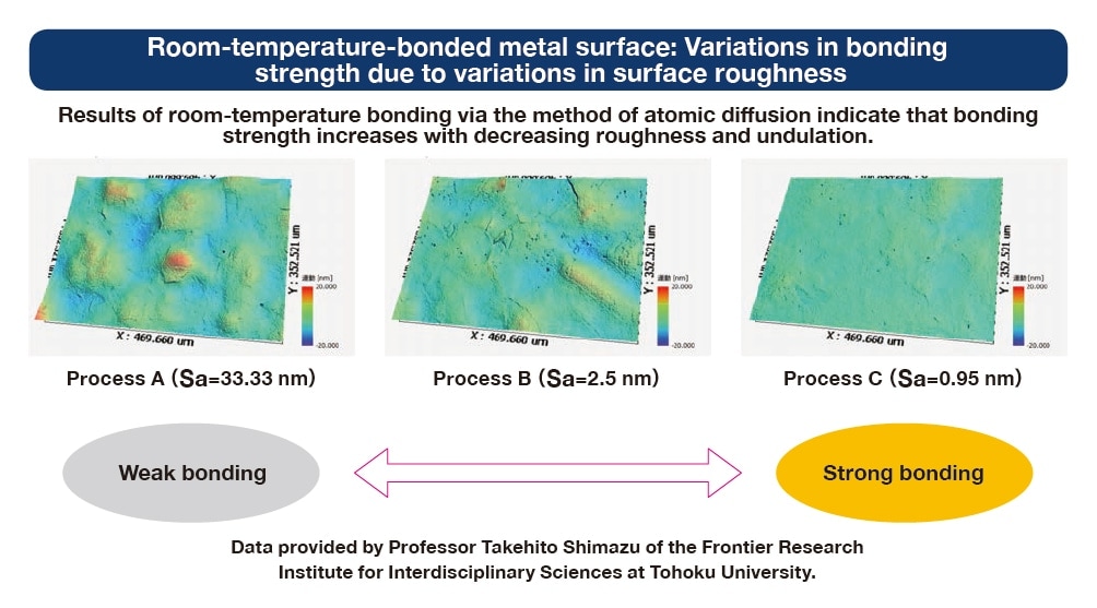
Fig. 3 A measurement case study from the field of room-temperature wafer bonding, indicating different bonding strengths for regions of different surface roughness.
In this section we use a real-world case study to discuss the ISO 25178 parameter-assistance capability included as a
standard feature of the VS1800.
In the past, surface-roughness controls were based on the Definitions and indicators of surface roughness established by the Japanese Industrial Standards Committee and distributed in the form of JIS standards; however, following the introduction of measurement instruments that promoted evolution from line measurements to area measurements, the Definitions and indicators of surface roughness evolved to reflect t he shift from l ine-based to area-based data. ISO 25178 is an alternative standard addressing “area roughness characterization,” conducted using instruments capable of area measurements, in contrast to earlier JIS and ISO standards premised on the assumption of “line roughness characterization” by contact-probe instruments.
The sample shown in Figure 4 is a high-gloss paper used to print photographs. We have chosen this sample as an example in which spatial variations in surface properties—despite being so significant that they are readily discernible by the naked eye—cannot be clearly quantified numerically by the line measurements considered in conventional JIS standards. In cases like this, a consideration of the surface-roughness parameter Sa (arithmetic mean height) defined by ISO 25178 allows determination of numerical values for sample-to-sample differences in surface roughness, a metric that is difficult to assess via line-based measurements; unfortunately, for the particular samples considered here (Figure 5), one finds that differences between samples are difficult to quantify numerically even when using the parameter Sa.
Thus, one would like to use another of the parameters defined by ISO 25178 to yield a clear quantification of discrepancies; however, to determine which of these many parameters is optimal for this purpose would require one to acquire numerical values for each parameter for all samples, then search this data set to identify the parameter yielding the greatest discrepancy—an enormous and highly complicated task. This procedure becomes particularly essential when comparing unknown samples, as opposed to samples for which the most appropriate parameters have been predetermined by agreement among previous researchers.
A useful tool for cases like this is the ISO 25178 parameter-assistance feature of the VS1800 (Figure 6). This feature acquires data for multiple comparison samples and sorts the results to identify the parameters with the greatest sampleto-sample variation. An application of this feature to the present case (Figure 7) required only a brief amount of time to conclude that, for these samples, the optimal parameter for characterizing discrepancies is Sdr (developed interfacial area ratio).
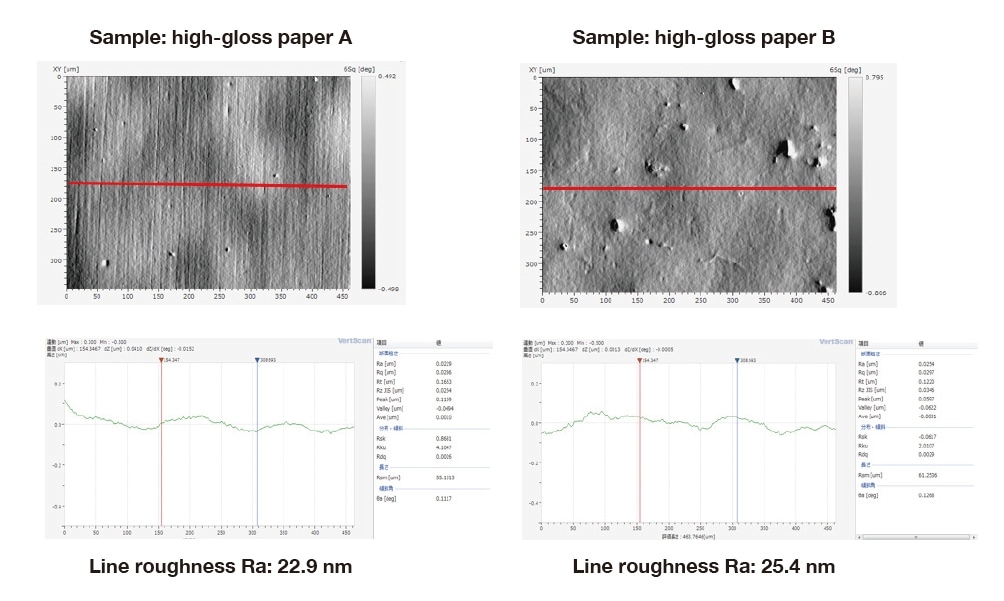
Fig. 4 An example of a case in which conventional standards fail to yield a clear quantification of sample-to-sample differences in roughness
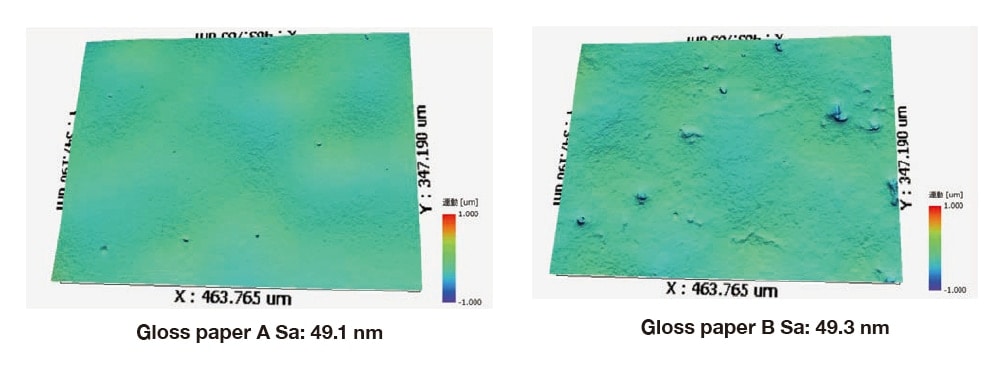
Fig. 5 Calculated surface-roughness parameter Sa for the samples of Figure 4
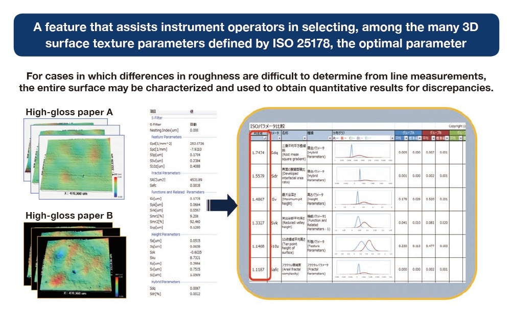
Fig. 6 The ISO 25178 parameter-assistance feature
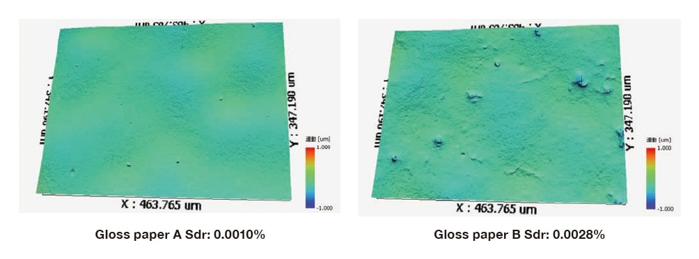
Fig. 7 Optimal parameter determination for the samples of Figure 4
The Nano 3D Optical Interferometry System VS1800 offers a unique feature option not available on other instruments: layer cross-sectional analysis. This feature allows non-destructive thickness measurements for all layers of a multi-layer film and non-destructive measurements of impurity depth positions.
Figure 8 shows a schematic illustration of this feature. When a double beam interference objective lens is scanned in the vertical direction above a multi-layer film sample, phase interference arises at the top surface, bottom surface, and layer-interface surfaces of the sample. By remembering the coordinates of the positions at which the intensity of this phase interference is maximized, one obtains not only surface-morphology data but also information on the state of thickness variations for each layer.
Figure 9 shows non-destructive measurements of surface morphology and cross section for a sample of adhesive tape consisting of a PET layer and an adhesive layer. The conventional procedure for characterizing this sample would be to prepare a cross-sectional sample of the tape for observation via scanning electron microscope (SEM); however, this method suffers from the problem of low image contrast due to damage to the observed surface incurred during the preparation of cross-sectional samples or charge deposition and elemental-composition gaps arising during SEM observation. In contrast, the use of layer cross-sectional analysis allows non-destructive measurement of layer thicknesses at arbitrary positions, as well as rapid determination of the depth positions of gas bubbles or impurities in the sample interior, avoiding the problems introduced by sample preparation or SEM analysis.
Note that, as of this writing, this unique capability for multi-layer film characterization is an exclusive feature of the Nano 3D Optical Interferometry System VS1800, not available on other instruments capable of making area measurements.
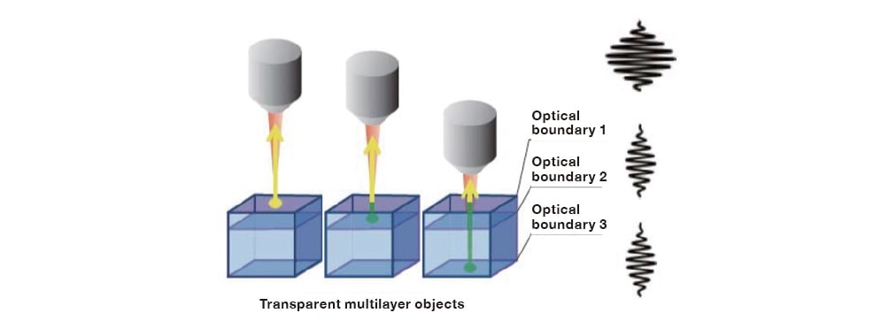
Fig. 8 Schematic illustration of film-thickness measurements
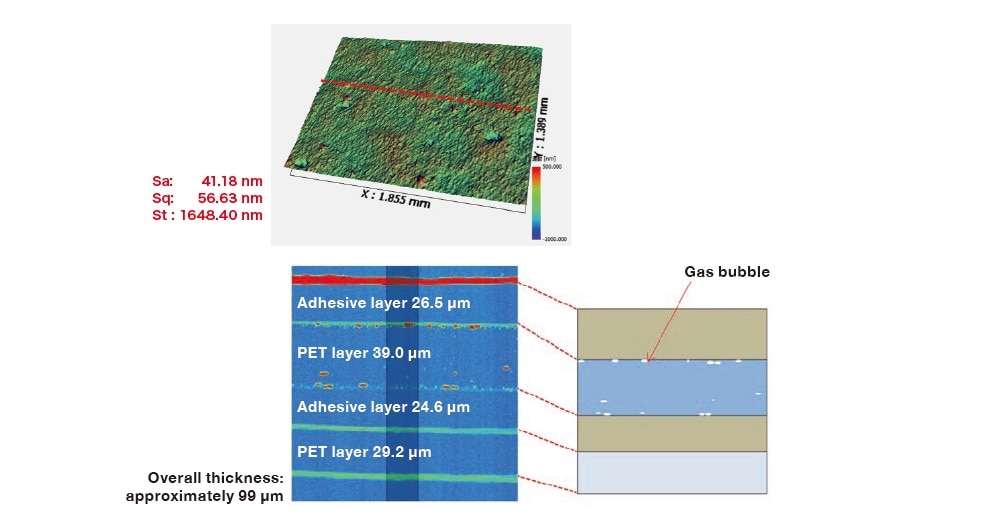
Fig. 9 Surface roughness and cross-sectional layer structure of a sample of adhesive tape containing a gas bubble
In this note, we surveyed recent developments in the field of surface metrology, then introduced a new instrument based on the recently developed method of CSI and discussed a number of application case-studies.
The evolution of surface-morphology measurements from contact-probe line measurements to non-contact area measurements, and from LSM techniques to a new generation of CSI instruments, is currently enjoying a moment in the spotlight due to the multi-angle analytical capabilities afforded by non-contact area measurements and their ability to yield highly accurate data in short periods of time, simultaneously realizing the dual goals of high productivity and high reliability.
Going forward, CSI-based instruments will be increasingly valuable tools not only for characterizing functional films and flat-panel displays, but also for tribology and other fields of material characterization that require highresolution measurements of wide sample areas; we also expect these instruments to become the tools of choice for a variety of surface-processing techniques. Hitachi is committed to providing instruments equipped with cutting-edge technology for use in cutting-edge settings, contributing to all sectors of Japanese manufacturing from the standpoint
of surface measurement.
Data Sources
Figure 3: Professor Takehito Shimazu, Frontier Research Institute for Interdisciplinary Sciences, Tohoku University.
Abbreviations
AFM: Atomic force microscopy
LSM: Laser scanning metrology
CSI: Coherence scanning interferometry
About the author
Junji Kuwahara
Metrology and Analysis Systems Division
Nano-Technology Solution Business Group
Hitachi High-Tech Corporation
See more
