Toru Aiso
In recent years, the use of low accelerating voltages in scanning electron microscopy (SEM) has made it possible to observe the outermost surface layers of samples while simultaneously using one or more additional detectors to acquire various types of information on the sample. One complication is that the SEM images are influenced by the choice of accelerating voltage and the use of additional detectors; thus, when interpreting acquired SEM images, one
must properly take into account the penetration depth of the irradiating electrons and the detection energy bands for the detectors. Scanning probe microscopy (SPM) instruments are no longer limited to measuring sample morphology, but now offer sophisticated capabilities for measuring a diverse range of physical properties of samples—including electromagnetic and mechanical properties. A third measurement method, coherence scanning interferometry (CSI), offers the ability to make non-contact, high-throughput measurements with sub-nanometer height resolution over wide sample areas—on the order of millimeters—and has become widely adopted for testing purposes at production facilities, although its spatial resolution is limited by the wavelength of light. Although each of these three
pillars of modern metrology—SEM, SPM, and CSI—is a formidable tool on its own, there are some problems that cannot be solved by any one technique in isolation; in such cases, a powerful strategy is the method of correlation analysis, a hybrid technique in which SEM, SPM, and CSI measurements of a single sample region are combined in complementary ways to exploit the strengths of each method and produce a deeper interpretation of measurement results. In September 2016, we at Hitachi introduced SÆMic (pronounced “same-ick”), a measurement solution combining SEM and SPM observations of identical sample regions; since that time, we have been working to add CSI into the mix as well.
In this article, we use a series of real-world case studies to introduce the method of SEM-SPM-CSI correlation analysis.
Scanning electron microscopy (SEM)
SEM uses magnetic and static electric fields in vacuum to focus an electron beam that irradiates the surface of the measurement sample; the beam is scanned over a region of the sample, and the secondary electrons and backscatteredelectrons resulting from this process are detected to generate images. SEM is frequently used in conjunction with other analytical methods such as energy-dispersive X-ray spectroscopy (EDX)—which analyzes characteristic X-rays
emitted during SEM measurements to perform elemental analysis—and electron backscatter diffraction (EBSD), in which crystal orientation and phase distributions are identified by electron-beam diffraction patterns.
As shown in Figure 1, most SEM instruments are equipped with multiple detectors; in general, both secondary electrons—which give information on the roughness of the sample’s outermost surface—and backscattered-electrons, which give information on sample composition, are detected, and the acquired images are interpreted accordingly. Although SEM in the past was used primarily for observation and analysis, in recent years it has become possible to make 3D measurements using segmented backscattered-electron detectors installed immediately beneath the objective lens (Figure 2), the importance of correlative analysis with SPM and CSI has been increasing.
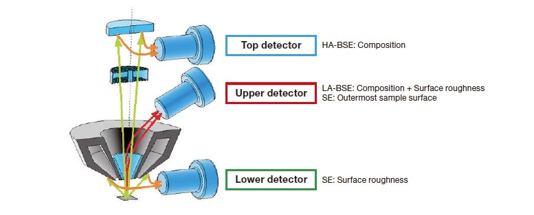
Fig. 1 Detector layout of the Regulus 8200 series of FE-SEM instruments.
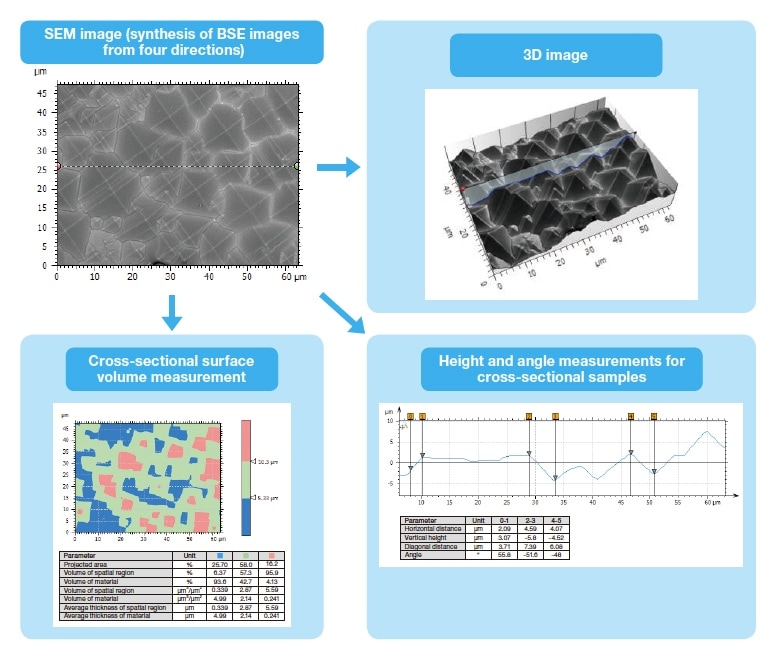
Fig. 2 3D measurement via tabletop SEM of the surface of a solar cell.
Scanning probe microscopy (SPM)
In SPM, a probe tip—sharpened to a tip radius on the order of a few nanometers—is mounted on a cantilever and scanned over the sample surface using a piezo scanner, measuring surface topography on length scales ranging from sub-nanometer to hundreds of microns. As shown in Figure 3, laser light scattered from the rear surface of the cantilever is collected by a photodetector to detect the microscopic forces produced by the interaction between the probe tip and the sample surface. The technique may also be used to detect various types of forces acting between the probe tip and the sample—including friction forces, viscoelasticity, magnetic forces, and electrostatic forces—and to measure conductivity and dielectric properties by using the probe tip as a kind of nanoprobe terminal.
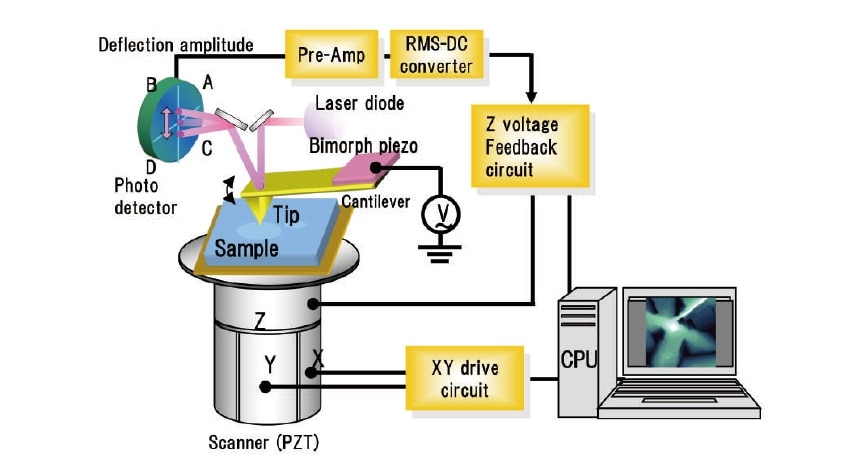
Fig. 3 Conceptual diagram of SPM.
Coherence scanning interferometry (CSI)
The principles of CSI are illustrated in the conceptual diagram shown in Figure 4. Light from a white-light source is split by a beam splitter into two components, of which one is directed to the sample surface while the other is directed to a reference surface. Upon recombining the reflected beams, interference fringes are produced—encoding differences in optical path length due to sample surface roughness—which may be converted into information on the height of the sample surface, thus measuring the 3D morphology of the sample. Also, as shown in Figure 5, by observing light reflection from each interface in a transparent multilayered structure, CSI offers the ability to make nondestructive cross-sectional measurements without the cumbersome process of preparing cross-sectional samples.
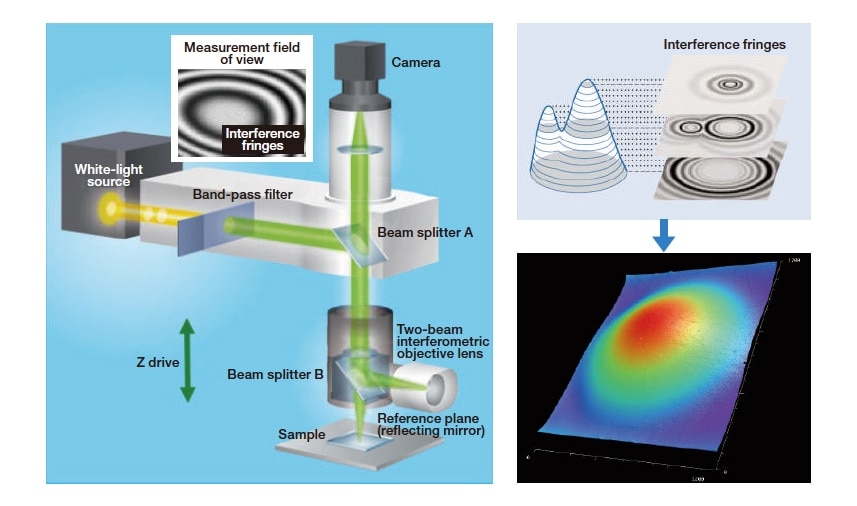
Fig. 4 Conceptual diagram of CSI.
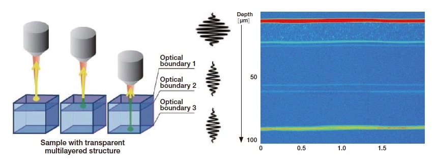
Fig. 5 Layered cross-sectional analysis: Conceptual diagram (left) and illustrative measurement of multilayer barrier film (right)
Correlation analysis requires that all instruments observe the same sample region. This condition is particularly easy to satisfy with Hitachi instruments, because some SEM, SPM, and CSI systems share a common feature—a high-precision motorized stage allowing acquisition of coordinate information (Figure 6). In particular, for SEM-SPM correlation analysis—a task which demands especially high resolution—it is only necessary to mount the sample in the dedicated sample holder, using its shared alignment markers; high-precision coordinate linkage is then ensured by the automated software-based stage alignment capabilities of the instruments. A key advantage of this strategy for combining SEM with SPM is that it does not constrain the performance or functionality of either—something that cannot be said for the alternative approach to hybrid SEM/SPM, in which an SPM is placed inside an SEM chamber.
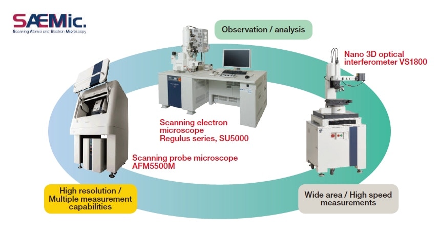
Fig. 6 Conceptual diagram of SEM-SPM-CSI linkage.
The separators used in lithium-ion batteries (LIBs) and similar devices are easily damaged by electron-beam irradiation, and thus SEM observations of separator samples require careful tuning of accelerating voltages and beam currents. SPM, of course, allows morphology measurements with no damage to the sample, but has limited throughput and is restricted to relatively small sample areas; thus, there is an urgent need for SEM systems capable of damage-free observations of large sample regions.
Figure 7(a-c) are SEM images, acquired at three different accelerating voltages, of a LIB separator sample; for reference, Figure 7(d) shows an SPM topography image of the same sample1). To minimize static charge and maximize clarity for SEM observations, the sample was coated with the static-charge-reducing ionic liquid IL1000 as a preprocessing step before SEM observations2). SEM images acquired at accelerating voltages of 0.5 kV and 1 kV show large sample defects that are not present in the SPM image, indicating that the separator sample suffered electronbeam damage at these voltages. Reducing the accelerating voltage to 0.06 kV yields a morphology image in agreement with the SPM results, suggesting that beam damage is avoided under these conditions. Although the SEM and SPM measurements in this case did not observe the same sample region, the images produced by the two methods indicate similar cross-check patterns in the sample morphology, making this an excellent demonstration of the correlation analysis.
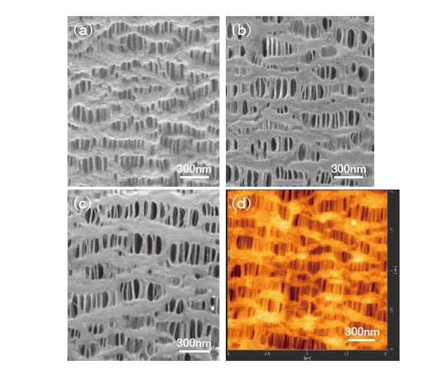
Fig. 7 (a-c) SEM images (×50k) of separator sample after IL1000 coating.
(d) AFM image of uncoated separator sample.
SEM accelerating voltages: (a) 0.06 kV, (b) 0.5 kV, (c) 1.0 kV
Detailed analysis of the factors responsible for degradation in LIBs under charge-discharge cycling is a central component of efforts to increase the performance and extend the lifetime of these devices. For an anode made from a graphite-SiOx blend, Figure 8 presents the results of a correlation analysis in which SEM-EDX measurements were combined with information obtained by scanning spreading resistance microscopy (SSRM), a measurement mode offered by the SPM system for characterizing electrical properties to study variations in the anode’s structure, elemental distribution, and electrical resistance distribution under three sets of conditions: before cycle tests, after cycling at room temperature, and after cycling at high temperature3). Thanks to the system’s environmentally isolated milling holder—a single, shared sample holder used for SEM, SPM, and ion milling—the measurement sample may be prepared and transferred from one instrument to another without exposure to the environment. While SSRM images acquired before charge-discharge cycling show relatively low resistance in regions near the outer perimeter of the graphite active material, in SSRM images acquired after room-temperature cycling and after high-temperature cycling, the boundaries of the active material are clearly discernible, indicating high resistance in this region. In post-cycling images, the presence of fluorine near the outer boundaries of the graphite active-material region and of the Si activematerial region—where the fluorine concentration is particularly high—suggest the formation of a solid-electrolyte interface (SEI) in these regions, explaining the increased electrical resistance observed there. SSRM has the advantage of capturing resistance distributions—with a wide range extending from 104 to 1010 Ω—after only a single scan. In this case, the combination of SEM-EDX with SSRM enables a powerful correlation analysis that clarifies one major contribution to the increased internal resistance of the battery.
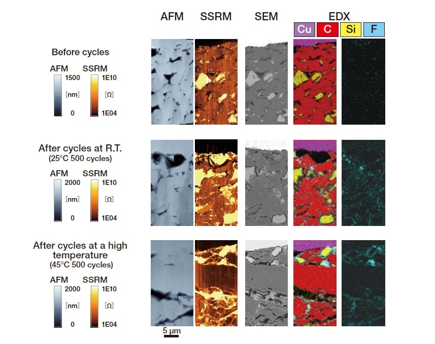
Fig. 8 Results of SSRM/SEM/EDX observations of a milled cross-sectional sample of a lithium-ion battery anode before and after charge-discharge cycling.
A widely used approach for analyzing the cross-sectional structure of samples is to use mechanical polishing, ion milling, or similar techniques to expose a cross-sectional surface of the sample, and then observe this surface via SEM. Although this strategy covers wide areas and allows high-resolution observations of the cross-sectional structure, the preparation of cross-sectional samples is time consuming, often requiring multiple hours per sample. Figure 9 shows the results of a case study in which a correlation analysis combining CSI for layered cross-sectional measurements with SEM for detailed cross-sectional observations was used to study the coating thickness of a cross-sectional surface of the welded portion of a beverage can4). The SEM image clearly reveals the cross-sectional structure—but preparing the cross-sectional sample for this observation required around two hours. In contrast, CSI obtains cross-sectional structures at arbitrary sample points, does so non-destructively, and requires only around 20 seconds to complete an observation for a single field of view. As the coating thickness obtained via CSI is comparable to the result of crosssectional SEM, we conclude that CSI is the better choice for cases in which measurement throughput is important.
Figure 10 presents a case study involving an impurity analysis of a transparent multilayered film5). CSI layered cross-sectional analysis reveals that impurities are present—at a depth of 109 μm below the surface—but does not determine the elemental composition of the impurities. For this purpose we use the μXRF (micro-X-ray fluorescence) tool provided by the SEM system, which irradiates the relevant sample region with 50 kV X-rays and uses the EDX detector to identify the composition of the impurities. This example illustrates how proper use of correlation analysis— in this case, combining CSI for cross-sectional screening with SEM for detailed analysis—enables highly efficient use of measurement time.
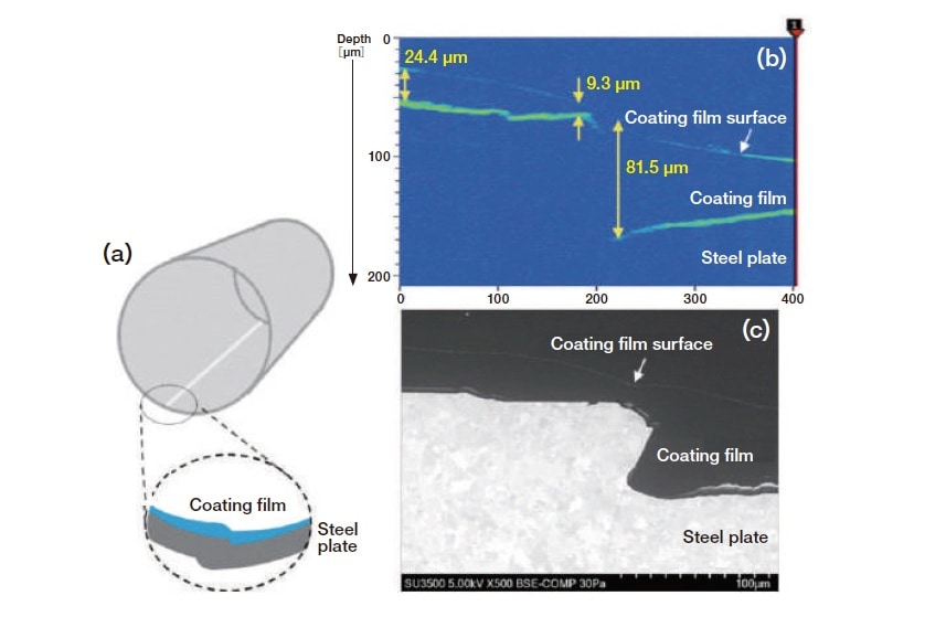
Fig. 9 (a) Schematic diagram showing welded portion of beverage can.
(b) CSI layered cross-sectional analysis image.
(c) Cross-sectional SEM image (5 kV, ×500, after ion milling of sample)
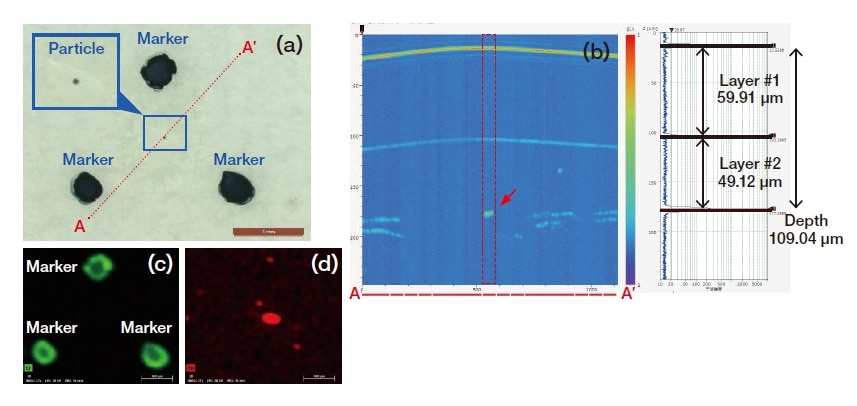
Fig. 10 (a) Optical microscopy image of layered film.
(b) CSI layered cross-sectional analysis image.
(c) Cr map (μXRF-SEM-EDX image) (d) Fe map (μXRF-SEM-EDX image)
When analyzing SPM-acquired physical-property data for the outermost surface of a sample, researchers often express wishes for some way to visualize the spatial extent—in the depth direction—of the portion that is influenced by surface phenomena. Figure 11 shows the results of a case study in which an aluminum alloy, following immersion
for 30 minutes in a 1% aqueous solution of NaCl to promote corrosion, was investigated by way of a correlation analysis in which 3D-SEM/EDX images obtained via FIB (focused ion beam)-SEM were combined with surface electric potential distributions analyzed via KPFM (Kelvin-probe force microscopy), another of the measurement modes offered by the SPM system for characterizing electrical properties6).
For this measurement, we make use of coordinate-linkage functionality to ensure that 3D-SEM/EDX images of the same sample region observed by KPFM are acquired via the Cut&See procedure—in which processing steps alternate with observations repeatedly—after which 3D-SEM/EDX and KPFM images are superposed to yield a compound image. From the SEM-EDX image, we see that Fe-based inclusions are present at the Al alloy surface, indicating oxidation of the surrounding sample region. The KPFM image shows that the surface potential is lower at Fe inclusion sites than in other regions and also low in oxidized regions. Such potential gradients are thought to be among the factors responsible for promoting corrosion, and KPFM measurements are useful for pinpointing sample regions at which corrosion is likely to spread. However, KPFM alone does not suffice to elucidate the progress of corrosion into
the sample interior. Instead, we performed FIB-SEM observations to clarify the distribution of elemental composition in the sample interior, as shown in Figure 12. The results reveal that oxygen—the signal of corrosion—has begun to penetrate the sample interior by way of Fe inclusion sites [Figure 12 (b)↑1]. On the other hand, Fe inclusions present in the sample interior but near the surface [Figure 12 (b)←2] do not affect the surface potential, suggesting that they are not yet involved in corrosion. These results demonstrate that the origins of the surface properties captured by A FM may also be investigated via the internal structure revealed by FIB-SEM.
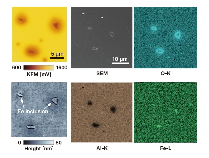
Fig. 11 Results of KFM/SEM/EDX measurements of a corroded Al alloy.
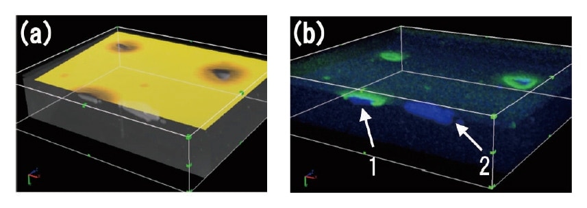
Fig. 12 (a) Overlay image of 3D-SEM with KFM data.
(b) 3D-EDX image (blue: Fe-L; green: O-K)
(1) Fe inclusions exposed to the outermost surface layer.
(2) Fe inclusions buried near the surface.
The case studies presented in this article demonstrate that the use of multiple instruments to analyze the same region of the same sample not only helps confirm data reliability, but also lends deeper insight into the interpretation of the data. The technique is useful for screening purposes and offers a range of other advantages as well.
In the future, we will remain enthusiastic promoters of correlation analysis as a problem-solving tool and pursue techniques for streamlining—and increasing the precision of—linkages between metrological techniques. We hope to design systems that make correlation analysis available and convenient for all researchers.
References
Publication data
Published in the monthly journal Engineering Materials (May issue 2020)
About the authors
Toru Aiso
Analysis Systems Solution Development Department
Metrology and Analysis Systems Product Division
Nano-Technology Solution Business Group
Hitachi High-Tech Corporation
See more
