Yoichiro Hashimoto*1, Hironori Itabashi*2, Tsutomu Saito*3
Recent years have witnessed increasingly urgent demand for lighter, stronger versions of the metallic materials used to make components for the automotive and aerospace industries. The strength of materials under tensile stress is thought to be heavily affected by microscopic structural factors such as crystal grain size, distortion, impurities and sedimentary deposits, and dislocations. Consequently, insight into the relationship between macroscopic mechanical properties and microstructure can furnish valuable input for the development of new metallic materials.
A powerful tool for observing the microstructure of metals is scanning electron microscopy (SEM), and specifically the analysis of backscattered electron (BSE) images, which offer the key advantages of composition and channeling contrast. In particular, the installation of a stress-test substage inside the SEM chamber enables in-situ observation of changes in the microstructure of materials subjected to applied stress. In this article, we present case studies illustrating in-situ observation of dynamic variations in the microstructure of metallic materials under tensile stress.
We conducted observations using Hitachi’s SU7000 FE-SEM system. The SU7000, which features a Schottky emitter and an objective lens employing a superposition of electrostatic and magnetic fields, is a versatile instrument whose capabilities span a broad range of metrological objectives, including high-resolution observations at low accelerating voltages, high-current EDX analysis, and high-speed EBSD measurements. Figure 1 shows the full SU7000 system and a schematic diagram of its signal detectors. As shown in Figure 1(b), the SU7000 is equipped with multiple signal detectors, whose distinct properties allow acquisition of different types of information. The system is designed to ensure that all of these detectors acquire signals at the same working distance (6 mm), eliminating the need to adjust measurement conditions based on individual detectors and enabling simultaneous acquisition of multiple signals.
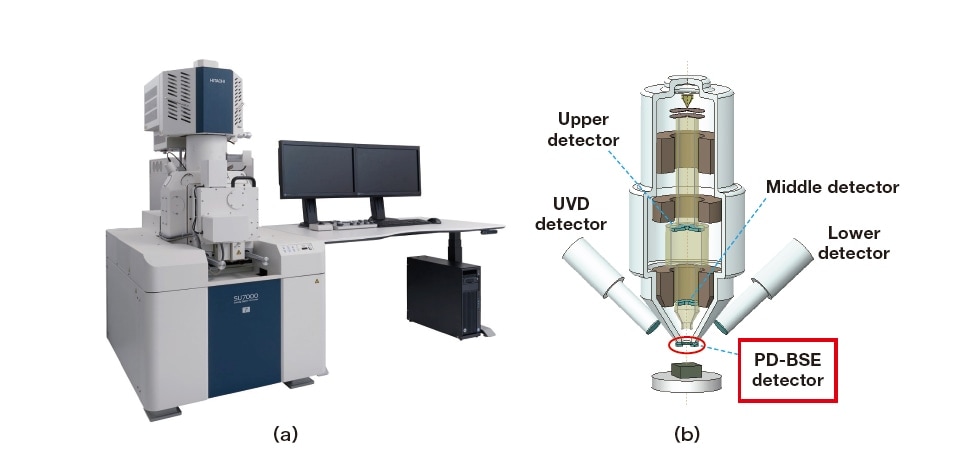
Fig. 1 The SU7000 Schottky FE-SEM. (a) Full system. (b) Schematic diagram of signal-detector subsystem.
We use the Deben Microtest300 tensile module to apply tensile stress. Figure 2 shows the Microtest300 installed on the sample stage of the SU7000, which features a standard draw-out specimen chamber to facilitate the incorporation of such specialized stages. For added convenience, the stage door is equipped with a feed-through port to simplify management of wires and cables.
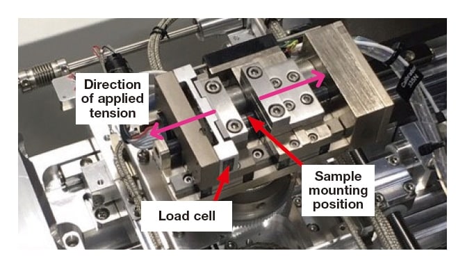
Fig. 2 The Microtest300 tensile module installed on the sample stage of the SU7000.
Photodiode BSE detectors (PD-BSEDs) excel at capturing composition and channeling contrast, and are a good choice for observations of the microstructure of materials. In-situ observations require instruments capable of acquiring images at high speed to ensure that dynamic responses to stimuli are captured in real time.
To enhance the quality of images acquired at high scan speeds, the SU7000 is equipped with a newly developed PDBSED whose response speed exceed that of existing detectors. Among the improved features of this detector is the possibility of applying reverse voltage biases to detector elements, as depicted schematically in Figure 3. Each PDBSED detector element consists of a semiconductor PN junction. BSEs impinging on the element create electron-hole pairs that migrate to the P and N layers due to the internal electric field in the depletion layer, constituting the detector input current. The application of a reverse bias voltage increases the depletion-layer width W, thereby reducing the parasitic capacitance C of the PN junction, which leads to an increased frequency bandwidth:
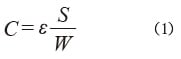
Here ε is the permittivity and S is the area of the element.
Increasing the depletion-layer width also has the effect of enhancing the rate at which electron-hole pairs are created, thereby increasing the magnitude of the detector current. The combination of these effects yields an overall improvement in detector response.
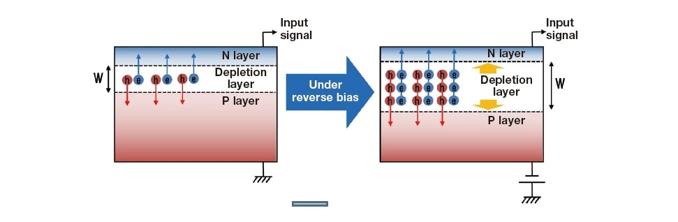
Fig. 3 Schematic depiction of effect of reverse voltage bias applied to PD-BSED element.
We conducted experiments to determine optimal experimental conditions for in-situ PD-BSED observation of a mechanically polished aluminum slab. We used an acquisition time 80 ms per frame and determined that the channeling contrast was optimized at an accelerating voltage of 3 kV. Figure 4 compares BSE images acquired under optimized conditions using (a) a conventional detector and (b) the SU7000 with the PD-BSED detector. The image captured by the conventional detector is blurry and does not clearly depict the microstructure of the material. In contrast, the SU7000 PD-BSED image clearly reveals both crystal grains—thanks to channeling contrast—and impurities, thanks to composition contrast.
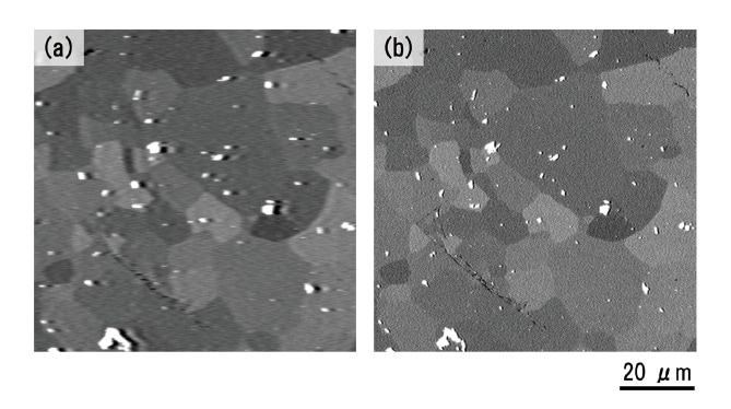
Fig. 4 Comparison of BSE images acquired during in-situ observations using (a) a conventional detector, (b) the PD-BSED detector of the SU7000.
We used the Microtest300 to apply tensile stress at a rate of 0.1 mm/min to an aluminum slab, and observed the process of the ensuing rupture. Figure 5 shows BSE images of the slab (a) before and (b) after rupture. In Figure 5(a), channeling contrast due to the crystal structure is clearly discernible. In particular, the channeling contrast exhibits especially prominent variation within the single crystal grain visible near the center of the field of view (dashed line); what we are observing here is the emergence of significant crystal distortion due to the application of tensile stress. In Figure 5(b) we see further progress of this crystal distortion near the ruptured cross-sectional surfaces, indicated by the reduced size of crystal grains.
Figures 6(b-j) show enlarged regions of snapshots taken from a movie of the rupture process. Figure 6(a) shows an image of the same sample region extracted from a larger image of a wide sample area captured prior to application of tensile stress. We see that the application of tensile stress has the effect of gradually reducing the size of crystal grains in the vicinity of grain boundaries [dashed lines in Figure 6(a, b)]. The images also provide in-situ observations of various stages in the rupture process, beginning with the formation of cracks [arrows in Figures 6(h, i)] along the boundaries of regions in which a reduction in crystal grain size occurs [dotted line in Figure 6(g)], culminating in eventual rupture.
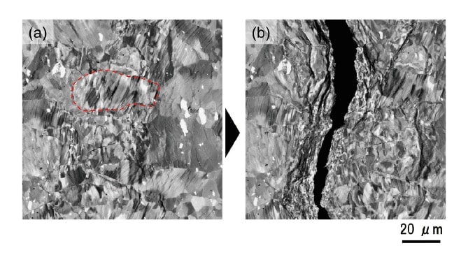
Fig. 5 In-situ SEM images of aluminum slab (a) before and (b) after rupture due to tensile stress.
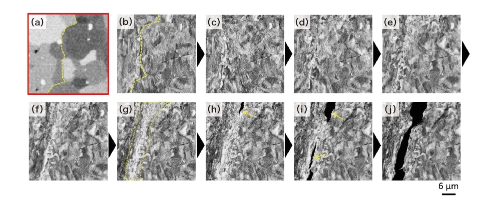
Fig. 6 In-situ SEM images of aluminum slab, extracted from a movie following the rupture process from the first application of tensile stress to the final rupture (accelerating voltage: 3 kV). Image (a) was acquired before the application of stress, while images (b-j) indicate various stages in the rupture process.
In this article, we presented a case study in which the SU7000 Schottky FE-SEM system and the Microtest300 tensile testing substage were used for in-situ observations of the microstructure of a metallic material subjected to tensile stress. Using a semiconductor-based backscattered electron detector with improved response properties, we investigated the optimal experimental conditions for observing dynamic structural variations induced by applied stress. Our observations clearly indicated reduced crystal grain sizes near grain boundaries and allowed visual tracking of the process of crack formation in these regions, ultimately resulting in rupture of the material. The metrological techniques presented here have the potential to yield new insights into the material properties and microstructure of metals, offering a powerful tool for the development of metallic materials.
Publication data
Published in the monthly journal Engineering Materials (April issue 2020)
About the author
Analysis Systems Solution Development Department
Metrology and Analysis Systems Product Division
Nano-Technology Solution Business Group
Hitachi High-Tech Corporation
Control Systems Design Department
Metrology and Analysis Systems Product Division
Nano-Technology Solution Business Group
Hitachi High-Tech Corporation
Electron Microscope Systems Design Department
Metrology and Analysis Systems Product Division
Nano-Technology Solution Business Group
Hitachi High-Tech Corporation
See more
