Microscopy Solutions for Semiconductors

Semiconductor scaling continues to this day at a remarkable rate. Now more than ever, cutting-edge technologies and techniques are being utilized to control device architecture at the atomic level. To this end, electron microscopy has proven to be an indispensable constituent of the industry because it allows for not only ultra-high-resolution imaging with a quick turnaround time, but also application on scales ranging from the package level to the atomic level required for the evaluation of controlled gate structures. Hitachi High-Tech provides the most advanced in-line analysis tools for semiconductor development and manufacturing as well as for failure analysis and quality assurance. Our expansive portfolio includes a wide range of microscopy solutions including ultrahigh-resolution FE-SEM, unique FIB-SEM systems, TEM, traditional SEM, and sample preparation equipment.
Products
Front-end R&D and Failure Analysis
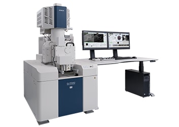
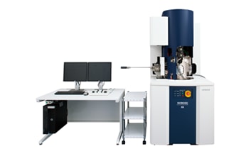
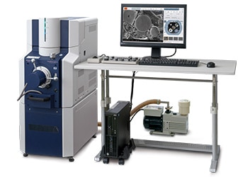
Ultra-High-Resolution Schottky Scanning Electron Microscope SU7000
SU7000: The Next-Generation FE-SEM
The modern FE-SEM requires not only high performance but also a multitude of functionalities including wide-area observation, in-situ analysis, variable pressure, high-resolution imaging at low accelerating voltages, and simultaneous multi-signal collection.
The SU7000 is designed to address these aspects and more by delivering enhanced information for diversified needs in the field of electron microscopy.
Experience the nano-world with the SU7000!
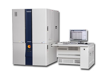
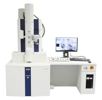
Ultra-high Resolution Scanning Electron Microscope SU9000II
The Cold Field Emission source is ideal for high-resolution imaging with a small source size and energy spread. Innovative CFE Gun technology contributes the ultimate FE-SEM with superior beam brightness and stability, affording high-resolution imaging and high-quality elemental analysis. Unique object lens design has a capability of EELS and diffraction as well.
High-precision FIB-SEM with Real-time SEM Observation
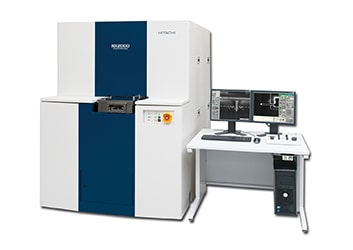
Hybrid FIB-SEM System NX2000
The ultimate TEM sample preparation tool
Cutting-edge devices for high-function nano-specimen evaluation and analysis, these tools offer functionality that only FIB-SEM hybrid technology can deliver.
Target structures are becoming more and more minutely detailed, increasing demand for TEM thin-film sample preparation systems that can prepare thinner, specimens free from artifacts.
Hitachi High-Tech has combined its established high-performance FIB and high-resolution SEM technology with attitude control and Triple Beam®*1 technology (optional) to produce the NX2000 series.
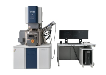
Focused Ion and Electron Beam System Ethos NX5000 Series
Unsurpassed Performance with Ultimate Flexibility
The Hitachi Ethos FIB-SEM incorporates the latest-generation FE-SEM with superb beam brightness and stability. Ethos delivers high-resolution imaging at low voltages combined with ion optics for nanoscale precision processing.
Real-time 3D analytical FIB-SEM NX9000
FIB-SEM System for True 3D Structural Analysis
The newly developed FIB-SEM system from Hitachi, the NX9000 incorporates an optimized layout for true high-resolution serial sectioning to tackle the latest demands in 3D structural analysis and for TEM and 3DAP analyses. The NX9000 FIB-SEM system allows the highest precision in material processing for a wide range of areas relating to advanced materials, electronic devices, biological tissues, and a multitude of other applications.
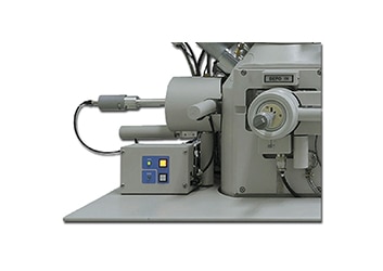
Micro-sampling System
This device is used for preparing the desired wafer part for analysis with STEM, TEM, etc. by extracting a micro sample with an ion beam in the vacuum chamber of an FIB system.
Sample Preparation and Cleaning
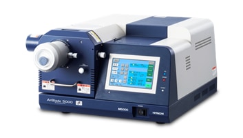
Ion Milling System ArBlade 5000
The most advanced broad ion beam system for producing exceptionally high-quality cross-section or flat-milling samples for electron microscopy.
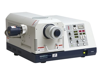
Ion Milling System IM4000Plus
The IM4000Plus Ion Milling System utilizes a broad, low-energy Ar+ ion beam milling method to produce wider, undistorted cross-section milling or flat milling, without applying mechanical stress to the sample.
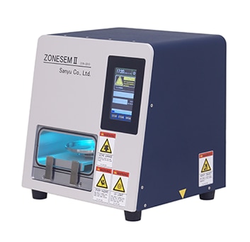
Sample Cleaner ZONESEMII
The ZONESEMⅡ。 Tabletop Sample Cleaner uses UV-based cleaning technology to minimize or eliminate hydrocarbon contamination for electron microscopy imaging.
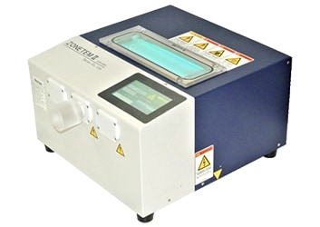
Sample Cleaner ZONETEM II
The innovative ZONETEM II Desktop Sample Cleaner uses UV-based cleaning technology to minimize or eliminate hydrocarbon contamination for electron microscopy imaging. ZONE offers easy-to-use cleaning for pre-analysis sample preparation, ensuring the best possible data from your TEM samples.
Conventional Imaging and Analysis
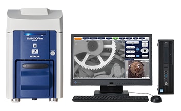
Tabletop Microscope TM4000 II / TM4000Plus II
The Future of Tabletop Microscopes is Here!
The TM4000 Series features innovation and cutting-edge technologies which redefine the capabilities of a tabletop microscope. This new generation of the long-standing Hitachi tabletop microscopes (TM) integrates ease of use, optimized imaging, and high-image quality, while maintaining the compact design of the well-established Hitachi TM Series products. Experience the new dimension of tabletop microscopes with the Hitachi TM4000 II and TM4000Plus II.
Scanning Electron Microscope FlexSEM 1000 II
The FlexSEM 1000 II VP-SEM combines innovative technological features with an intuitive interface, to deliver adaptability and flexibility in a powerful, automated, lab-friendly package. Cutting-edge technology and circuitry provides unrivaled imaging performance, even in variable-pressure environments, a feature previously only available in a full-sized SEM. This SEM runs on clean energy for an economical analytical tool, without compromising performance.
The FlexSEM will change your view of electron microscopy!
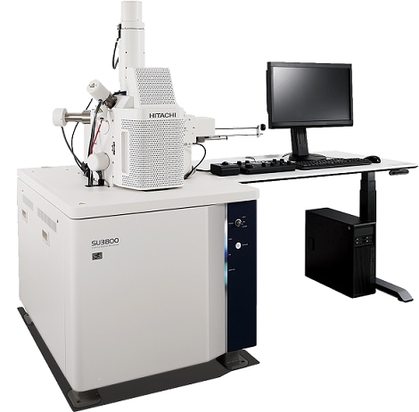
Scanning Electron Microscope SU3800/SU3900
Performance & Power in a Flexible Platform
Hitachi High-Tech's scanning electron microscopes SU3800/SU3900 deliver both operability and expandability. The operator can automate many operations and efficiently utilize their high performance. The SU3900 is equipped with a large multipurpose specimen chamber to accommodate observation of large samples.
High-resolution TEM / STEM for Composition & Defect Identification
Transmission Electron Microscope HT7800 Series
From biomedicine to nanomaterials
The NEXT Generation of Innovation. Meeting and Exceeding Needs and Requirements in Many Fields.
The HT7800 RuliTEM is a 120 kV transmission electron microscope (TEM) with multiple lens configurations, including a standard lens for unsurpassed high contrast and a class-leading HR lens for high resolution.
This breakthrough in advanced innovative design allows for highly efficient workflows and many specialized applications. It represents the cutting-edge solution for modern TEM analyses.
(Left image: Optional accessories included, the screen shows embedded TEM GUI)
Related Information