Sustainability
From smartphones and computers to consumer electronics and automobiles, and even online systems for businesses and national and local governments — semiconductors are indispensable for all kinds of products and services that support our daily lives.
Semiconductors are also essential in the digital transformation (DX) and green transformation (GX) for a sustainable future, so demand for them will continue to grow.
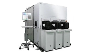
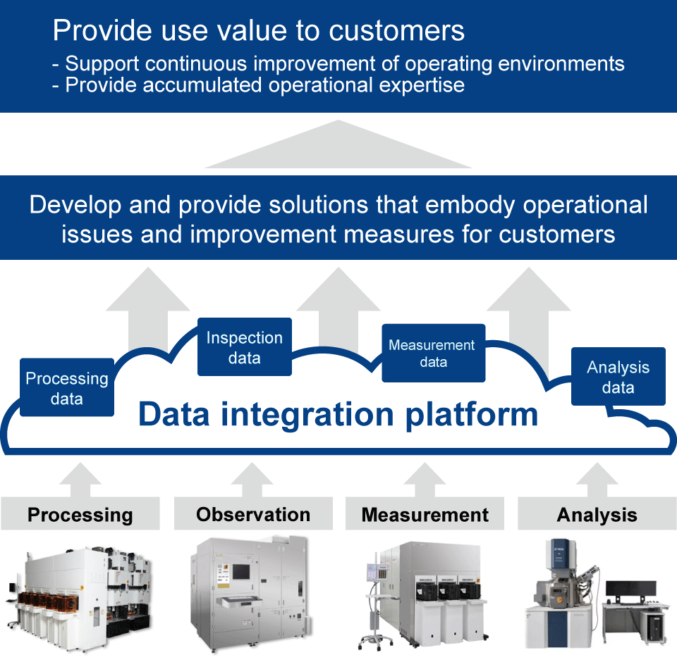
These manufacturing sites are supported by the measurement and inspection equipment for semiconductor manufacturing provided by the Nano-Technology Solution Business Group. The increasingly advanced demands are met by Hitachi High-Tech's high-precision plasma etching technologies, as well as the inspection, measurement and analysis solutions based on the company's core technologies of "Observation, Measurement and Analysis."
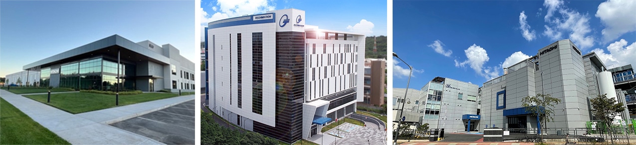
Also, by establishing new customer co-creation sites in North America, Taiwan and South Korea, thereby reducing the distance to semiconductor manufacturers, we are able to quickly solve problems and create new value. We will continue to contribute to the sustainable development of the semiconductor industry that supports our evolving digital society.
Semiconductors, which are often referred to as an industry staple, have become indispensable devices in our increasingly digitalized society. The global semiconductor market is expected to continue to grow at a rate of 9% (*), so the demand for the equipment that supports these manufacturing sites will be also expanded.
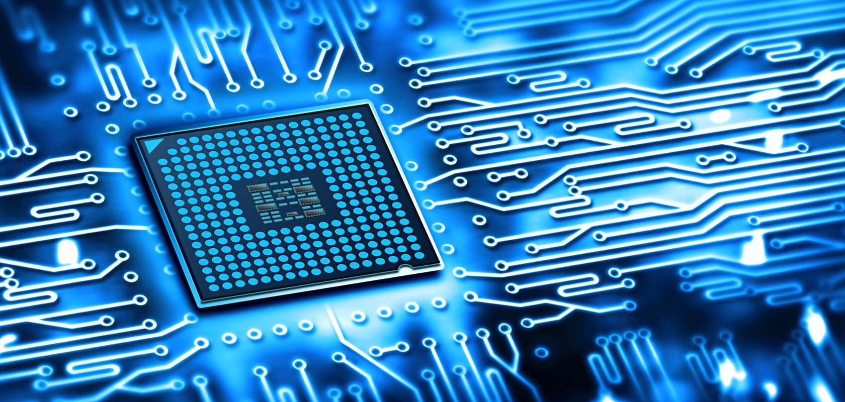
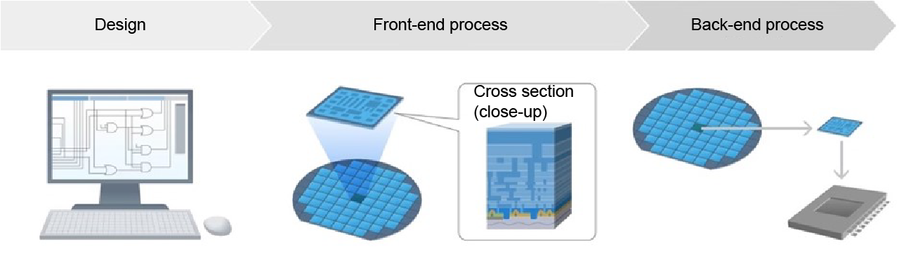
The term "semiconductor" generally refers to a semiconductor chip. It is an electrical circuit that consists of numerous transistors and wiring formed on a silicon wafer, and is sometimes referred to as an integrated circuit (IC) or a large-scale integration (LSI).
The manufacturing process of semiconductors is largely divided into three parts: the designing of the circuit; the front-end process, where the designed circuit is processed on a silicon wafer surface; and the back-end process, where the semiconductor chip is cut out and assembled into the product in a ready-to-use state.
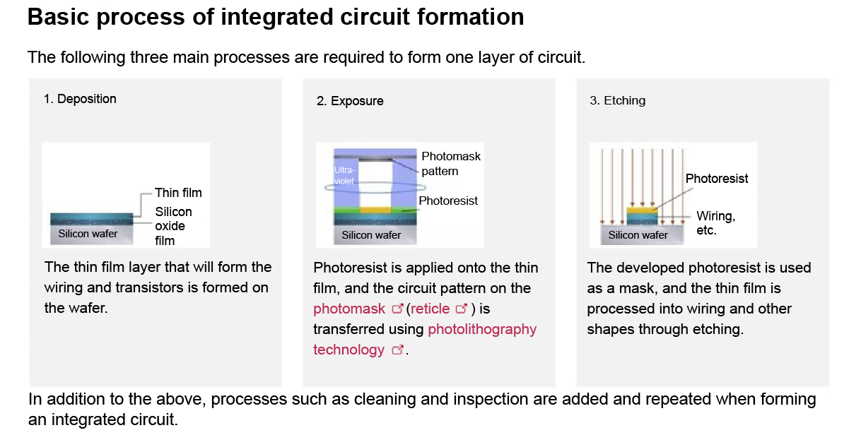
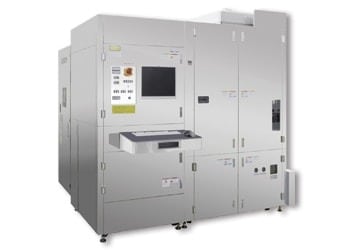
In addition, the front-end process is divided into three parts: deposition, exposure and etching. Among these, Hitachi High-Tech supplies manufacturing equipment for the etching process. Etching is a process whereby film is removed following a circuit pattern transferred onto a thin film on a wafer, before being processed into the actual wiring shape.
Hiroto Ohtake of the Semiconductor Manufacturing Systems Div., Nano-Technology Solution Business Group, explains the characteristics of Hitachi High-Tech's etching systems.
"Hitachi High-Tech is the only company in the world to supply etching systems that use Electron Cyclotron Resonance (ECR). ECR is a technology used for removing the film using artificial plasma, and is also compatible with cutting-edge miniaturization. It minimizes damage to the film, improving quality and yield."
So just how miniature is Hitachi High-Tech's "cutting-edge miniaturization"? Takayuki Mizuno of the Metrology Systems Div. explains, "Accuracy at the single-nanometer level is now expected."
"With a 100-nanometer level semiconductor device, an error of plus or minus one nanometer affects the performance of the device by about 1%. However, if it is a 4- or 5-nanometer level semiconductor device, the same 1-nanometer error will affect the performance by more than 10%. This discrepancy is crucial: as semiconductor applications such as artificial intelligence (AI), autonomous driving and robotics become more advanced, requirements are also becoming stricter."
The manufacture of semiconductors requires a level of quality control and inspection systems where not even the slightest defect or error is tolerated. This is where equipment that performs highly accurate inspection, measurement and analysis of integrated circuits really comes into its own. Hitachi High-Tech's core technologies of "observation, measurement and analysis" provide a one-stop solution for carrying out these processes.
Particularly in the field of measurement, Hitachi High-Tech's CD-SEMs (Critical-Dimension SEMs) continue to dominate the industry with a global market share of approximately 70% (*). These systems play a key role in measuring dimensions using electron microscope technology, and our latest models can measure dimensional errors right down to the 0.1 nanometer level.
In this way, Hitachi High-Tech provides etching systems that use our proprietary technologies, as well as comprehensive solutions that include "Observation, Measurement and Analysis." By making full use of AI and feeding back data gathered by the equipment to our customers, we are developing a portfolio that will help solve problems even at manufacturing sites.
Semiconductors are a strategic priority for many countries and regions, including Japan, so competition among semiconductor manufacturers is intensifying. As a result, the ability to respond to the wide range of issues that may occur at manufacturing sites has become a key area, says Hiroto Ohtake.
"In recent years, there has been a growing demand for cost reduction and increased speed, as well as improved quality. In order to meet this demand, it is crucial that we work with customers to reflect on the manufacturing process workflow. There is a strong demand for us to go above and beyond our role of a simple equipment manufacturer, and to change our mindset to that of a partner that works alongside customers to solve problems and create manufacturing sites."
In order to respond to increasingly stringent demands from customers, Hitachi High-Tech will establish new customer co-creation sites in North America, Taiwan and South Korea, which are all global semiconductor production centers. Construction of the locations in North America and South Korea was completed in 2022, and the aim is for the Taiwan location to begin operation in 2023.
Takayuki Mizuno has the following to say about the significance of establishing bases in these regions.
"Moving closer to our customers lets us build deep collaborative relationships and create and provide new value. For example, previously we had to transport wafers to Japan in order to carry out inspection and measurement demonstrations. The benefit of having a local presence is immeasurable, as it significantly reduces the time and effort spent on transporting people and products."
In recent years, power consumption has been reduced through the use of power semiconductors with highly efficient energy conversion. At the same time, reducing energy consumption and CO2 emissions at manufacturing sites are also important issues.
In order to meet these demands, Hitachi High-Tech is developing power-saving equipment while working to decarbonize its own sites where the equipment is produced.
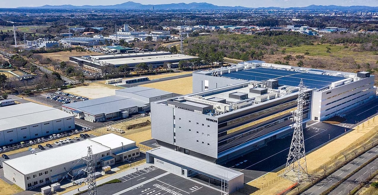
In March 2021, the construction of Marine Site (Hitachinaka City, Ibaraki Prefecture), a new development and manufacturing location for semiconductor manufacturing equipment, was completed. The site has been carbon-neutral since it began operation through the use of renewable energy sources such as solar power.
Hitachi High-Tech Group has formulated five materialities (key topics) for solving social issues, based on SDGs.
Semiconductor manufacturing, measurement and inspection equipment is particularly relevant to 1) and 3). Hitachi High-Tech Group aims to achieve carbon neutrality at all of its business sites by FY2027, a goal that the Marine Site has already managed to achieve.
In addition, we have introduced environmentally friendly designs and life cycle assessments in order to provide equipment with low power consumption and reduced environmental impact. Through this, we will contribute to decarbonization of the entire supply chain by reducing CO2 emissions at all stages — from the design, development and manufacturing of equipment all the way through to customer use.
For 3), as previously explained, we will respond to demands for increasingly sophisticated manufacturing sites by making full use of our core technologies of observation, measurement and analysis, and support the sustainable development of the semiconductor industry.
Semiconductors made with equipment supplied by Hitachi High-Tech are used in renewable energy such as solar and wind power, electric vehicles, and data centers that are key to digital transformation (DX), so they also contribute indirectly to 1) and 3).
The 2020 COVID-19 pandemic made contactless processes and remote working a lot more accessible. As further economic and industrial reforms are required to live in harmony with the global environment, society will continue to digitalize, and the demand for semiconductors will be higher than ever before. Hitachi High-Tech aims to continue to support semiconductor manufacturing sites and contribute to creating a sustainable future.