
Sustainability

It is no exaggeration to say that providing society with products that are in harmony with the environment has become the responsibility of manufacturing companies in recent years. Reducing environmental impact throughout the entire product life cycle—from procurement of raw materials to manufacturing, distribution, use, disposal and recycling—contributes to solving global issues such as climate change, scarcity of water resources, and environmental pollution caused by waste.
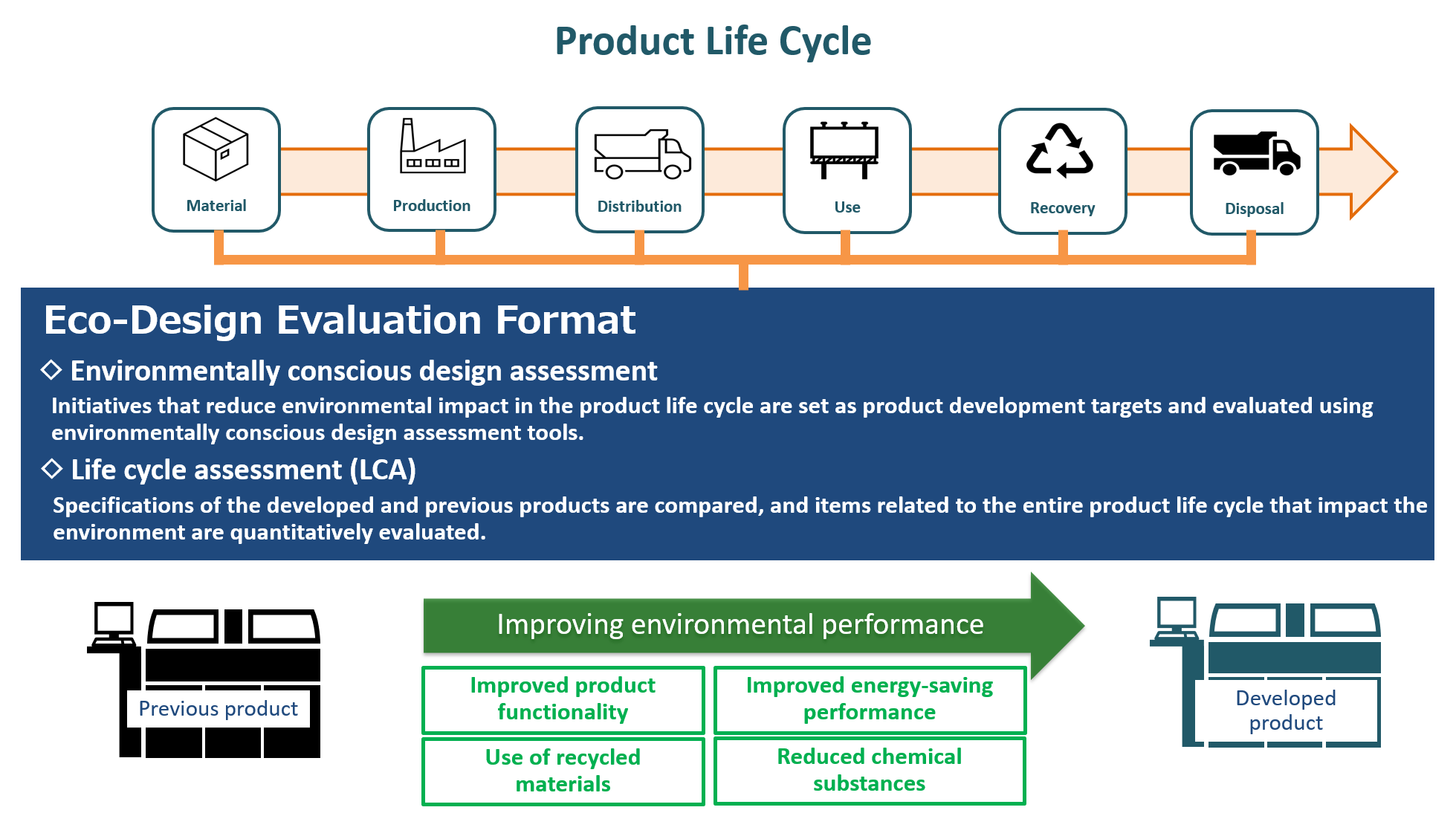
Hitachi High-Tech is promoting eco-design throughout the entire Group, with the aim of creating designs that are considerate of the environment right from the initial stages of product development, and quantitatively evaluating their environmental impact through LCA (Life Cycle Assessment).
One of the key elements of this initiative is our global target of reducing CO2 emissions, which is required to achieve carbon neutrality by 2050. Hitachi High-Tech has been promoting manufacturing with lower CO2 emissions by leveraging its unique technologies and expertise cultivated in the course of manufacturing over the years.
As an example of eco-design, we will look at the High-Precision Electron Beam Metrology System GT2000, the latest model of Hitachi High-Tech's flagship CD-SEMs. A CD-SEM is a metrology tool that measures the quality of semiconductor device patterns formed on silicon wafers at the nanometer-level,* making it indispensable to semiconductor manufacturers all around the world.
The latest CD-SEMs possess processing capabilities increased by 25% compared to previous models, while also having reduced CO2 emissions by 50% when compared to our standard product from FY2010. By achieving both improved measurement performance and greatly reduced environmental impact, Hitachi High-Tech is providing robust support to the rapidly expanding semiconductor market that is being driven by advances in generative AI, autonomous driving, next-generation communications and quantum technologies.
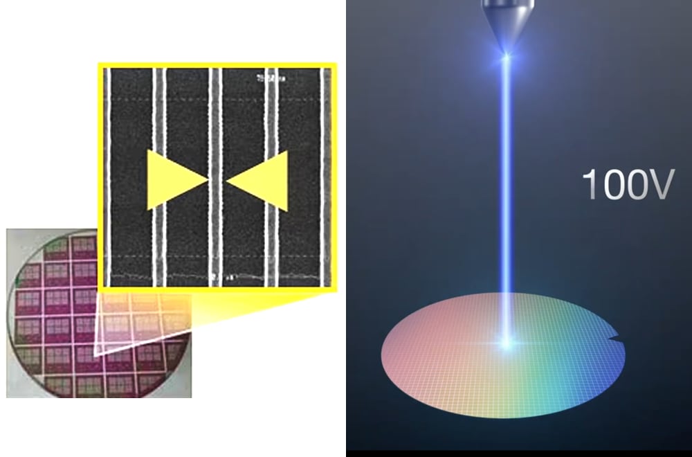
A CD-SEM can performs high-precision measurement of the dimensions of integrated circuits and other patterns formed on silicon wafers in the semiconductor manufacturing process in order to check whether these patterns have been produced according to the intended design.
These systems play a key role in measuring dimensions in semiconductor device manufacturing, and their contribution to increasing productivity through quality control and process optimization has made them indispensable to semiconductor manufacturers.
Measurement of semiconductor devices requires extremely high precision. For example, inside the latest smartphones, integrated circuits measuring just one square centimeter have more than 10 billion transistors and wiring patterns formed on them at nanometer intervals.
In the 2010s, the smallest unit in pattern design was 10 to 15nm. The performance required of semiconductors has rapidly increased since then, with the norm now being 2 to 3nm. To provide this increased performance within a limited space, devices are now stacked in layers of dozens or even hundreds of layers in a three-dimensional manner.
CD-SEMs are indispensable due to the ever-increasing miniaturization and complexity of semiconductor devices in manufacturing sites. SEMs, or Scanning Electron Microscopes, use the electron microscope technologies that the Hitachi Group have been developing for more than 80 years.
An electron microscope is a type of microscope that enables observation at the molecular and atomic levels by using an electron beam, which has a shorter wavelength than light. Using this technology, the CD-SEM scans semiconductor devices with an electron beam and performs measurements based on the images it acquires.
Since launching the world's first CD-SEM in 1984, Hitachi High-Tech has maintained a leading global market share of approximately 70%.
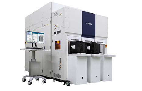
At the end of 2023, Hitachi High-Tech launched GT2000, its latest CD-SEM. Shusaku Maeda, Senior Engineer in the Electron Beam Systems Design Dept., explains the features of the new model.
"GT2000 was developed with eco-design firmly in mind right from the conceptual phase. By rethinking the design from scratch, we have achieved a combination of superior performance as a CD-SEM capable of achieving high-speed, stable measurements down to the 2nm level, together with high environmental performance. As a result, we were able to reduce CO2 emissions throughout the entire product life cycle by 50% compared to our standard product from FY2010."
GT2000 provides a 25% higher throughput compared to previous models. Throughput refers to the number of wafers that can be measured within a specific period of time. In other words, GT2000 can measure 1.25 times more wafers than previous models within the same amount of time and with the same power consumption.
Tomotaka Shibazaki, Engineer in the Metrology Product Design Dept., explains the key to improving throughput.
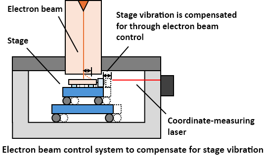
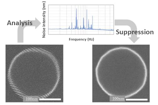
"In CD-SEMs, semiconductor wafers are loaded into a unit called a stage, and images are acquired by moving the stage to the desired coordinates to measure pattern dimensions. To increase throughput, the stage's movement speed must also increase. However, since nano-level measurement precision is required, vibration and electrical noise must be eliminated as much as possible."
Shibazaki continues,
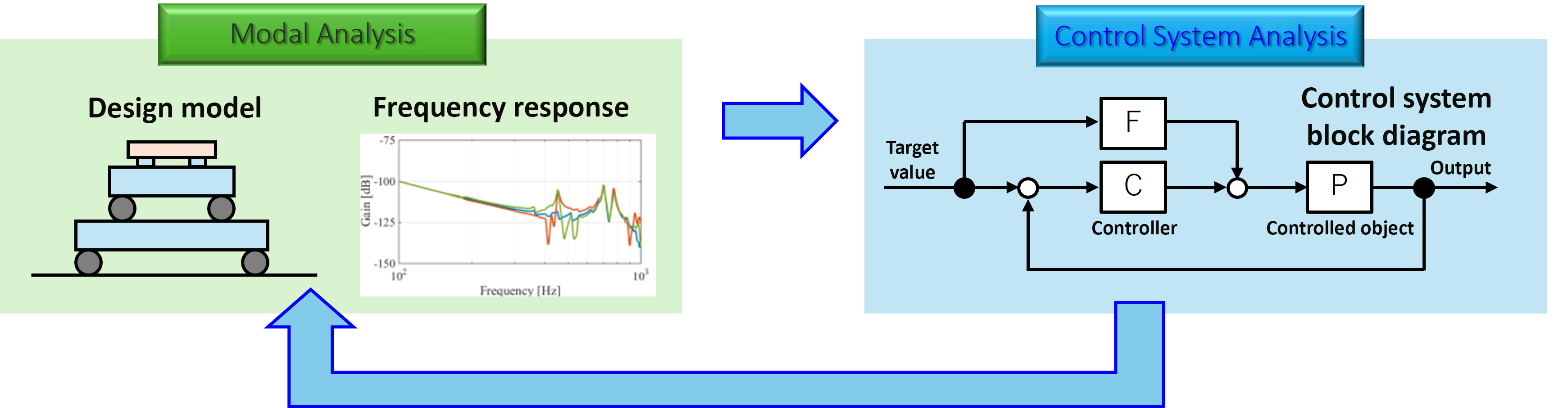
"This is why conventional stages were designed to reduce vibration by turning off servo control via the motor and applying brakes each time an image was acquired. To reduce the time required for each and every braking operation by tens of milliseconds,* GT2000 features Hitachi High-Tech proprietary control and measurement technologies that are finely aligned, thereby allowing the system to perform these high-precision measurements without braking. In addition, we have been able to achieve the optimal structural and control designs by leveraging analysis technologies cultivated by the Hitachi Group, enabling us to increase the movement speed of the stage itself, which also contributes to this increased throughput."
The 50% reduction in CO2 emissions was achieved through promoting energy efficiency and innovative tool design that has achieved an approximately 20% reduced footprint compared to previous model. One of the technologies that made this possible was the adoption of the compact, lightweight and highly efficient switch-mode power supplies. This power supply method is commonly used in devices such as smartphone chargers and laptop adapters.
Tomoyo Sasaki, Senior Engineer in the Metrology Systems Control-System Design Dept., explains,
"Although switch-mode power supplies contribute to miniaturization, weight reduction and energy efficiency in a variety of electronic devices, one drawback is that they are prone to generating noise.* For this reason, we had been avoiding using switch-mode power supplies in the development of highly noise-sensitive CD-SEMs, where measurement performance is the most important factor."
"However, we eventually came to think that using a switch-mode power supply was the only way to achieve our eco-design goal. So, we were faced with the most challenging technical issue in the electrical design of a CD-SEM—the issue of how to suppress noise to an acceptable level."
Sasaki continues,
"We started developing our noise analysis technology alongside the development of GT2000, as we believed that understanding complex noise phenomena correctly was essential to suppressing it. As a result of our persistent efforts to understand noise while refining our Power of Knowledge, we were able to develop and implement an electron beam control system that would suppress the impact a switch-mode power supply has on noise. We believe that this marked a major turning point in the history of CD-SEMs."
GT2000 systems are manufactured at Naka-Marine Site in Ibaraki Prefecture, a smart factory with cutting-edge environmental performance. The factory uses renewable energy sources, including solar power, to achieve virtually zero CO2 emissions during the manufacturing process.

"In addition, for the first time in CD-SEM development, we implemented simulations using mixed reality (MR) technology during the design stage of GT2000. This enabled us to reduce the number of prototypes produced from the conventional multiple iterations to just one, significantly reducing the amount of materials required during prototyping and thereby contributing to reducing CO2 emissions," adds Maeda.
Eco-design has also established a wide range of environmental criteria in addition to reducing emissions CO2, including resource conservation and being conscious of biodiversity. GT2000 has improved environmental performance through a variety of ways, such as its design that features long-life components and offers improved maintainability, as well as through the use of non-CFC cooling units.
"Some semiconductor factories deploy hundreds of CD-SEMs, so the benefits of improving the environmental performance of each and every unit are substantial. As social issues such as climate change have moved to the forefront over the past few years, I've experienced first-hand how consideration for the environment has come to be strongly demanded by society as a whole, including end users," says Maeda.
The Hitachi High-Tech Group has formulated five Sustainability Focus Areas (Materiality) for solving social issues, based on SDGs (Sustainable Development Goals).
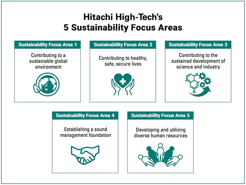
Entering a new generation through eco-design, CD-SEMs are deeply related to Focus Area 1 "Contributing to a sustainable global environment" and Focus Area 3 "Contributing to the sustained development of science and industry." It is fair to say that CD-SEMs contribute to all five focus areas. These systems are also related to Focus Area 2 in terms of supporting semiconductor manufacturing sites, which are essential to the digitalization of society, as well as being related to Focus Areas 4 and 5 as Hitachi High-Tech's mainstay products.
The three individuals involved in the development of GT2000 each speak about their commitment to the future.
"We believe that contributing to solving social issues is an important mission for Hitachi High-Tech. Our CD-SEMs undergo complete model refresh every five to seven years, with the successor model of GT2000 scheduled to be on the market by around 2030. Through product development, we will continue to strive toward our common goal of realizing a sustainable society and work together in unison throughout the company to create solutions that will change the future," says Maeda.
"CD-SEMs are a composite of various elemental technologies, such as mechanical design and electronics, and so they cannot be developed without the teamwork of engineers from each field. We will continue to strengthen our collaboration and explore what each of us as individuals can offer as part of this," says Shibazaki.
"Looking ahead to the future, ultra-precision CD-SEMs—which play a key role in measuring dimensions—will require electron beam control so precise that even atom-size vibrations or noise cannot be allowed. At the same time eco-design is becoming more and more essential. We will continue to take on new challenges in high-level technology and product development backed by our conviction that both goals can be achieved" says Sasaki.
As applications such become increasingly sophisticated, particularly with progress made in AI, the miniaturization of semiconductors too progresses. By around 2030, semiconductors are expected to become smaller than even nanometers and reach angstrom levels (0.1 nanometer).
Looking more broadly across society, some countries, local governments and businesses have started to champion carbon negative initiatives, whereby more CO2 is absorbed than is emitted, as well as nature-positive approaches that help restore natural environments. Digital transformation (DX) will play an essential role in achieving these ambitious targets as demand for semiconductors continues to grow.
We will continue to further improve our eco-design CD-SEMs in order to play a part in realizing an abundant, sustainable future.