
SEMICON JAPAN/APCS 2025
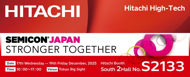
Hitachi High-Tech
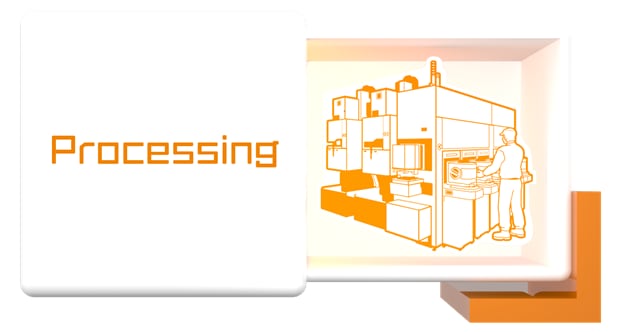
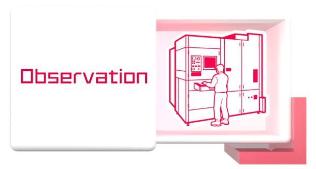
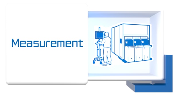
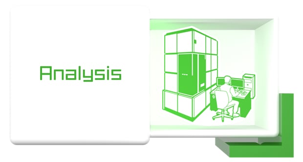
Hitachi High-Tech supports semiconductor manufacturing from the fundamental aspect of 'knowing' through technologies that "Processing, Observation, Measurement, and Analysis".

Hitachi High-Tech Corporation
Hitachi High-Tech Fielding Corporation
Date
December 17-19, 2025
10:00am – 5:00pm
Venue
Tokyo Big Sight
Organizer
SEMI Japan
Entrance Fee
Exhibition: Free need to register
Seminar : Partially Paid
Hitachi High-Tech Group Booth
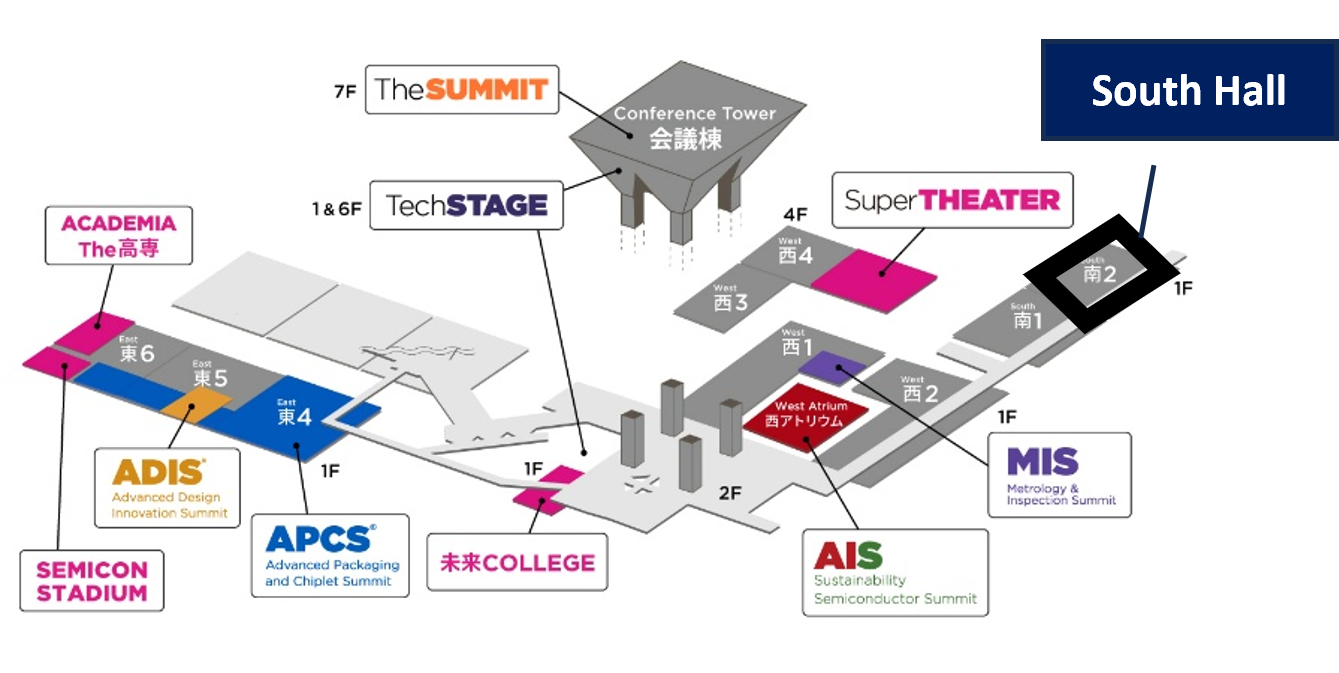
South Hall Hall 2:S2133
Exhibitor seminars (Free)

Date
Dec. 18 13:30~14:20
Venue
West Hall2 / West Hall2 Meeting Room (2) Private space (EXHIBITOR'S TechSPOT)
Theme
"Introduction of a new High-Resolution CD Measurement SEM CS5000 for High-Precision CD Measurement"
Hitachi High Tech has developed the CS5000, a successor to the high-resolution CD-SEM CS4800 for a wide range of 4, 6, and 8 inch wafers, featuring new optical modes capable of handling insulator wafers. This seminar will introduce and demonstrate the new CD-SEM CS5000.
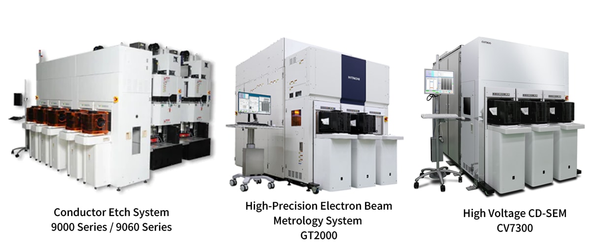
Exhibition Products
Hitachi High Resolution FEB CD Measurement SEM CS5000
Sustainable Maintenance Support
For details, please check Web page of SEMICON Japan 2025.