


SEMICON JAPAN 2026
SEMICON JAPAN Event Overview

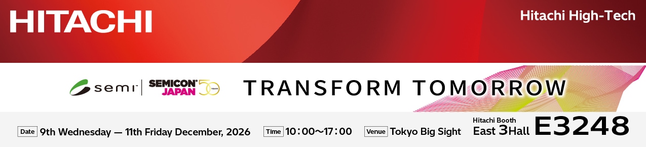
Date
10:00am – 5:00pm, December 9-11, 2026
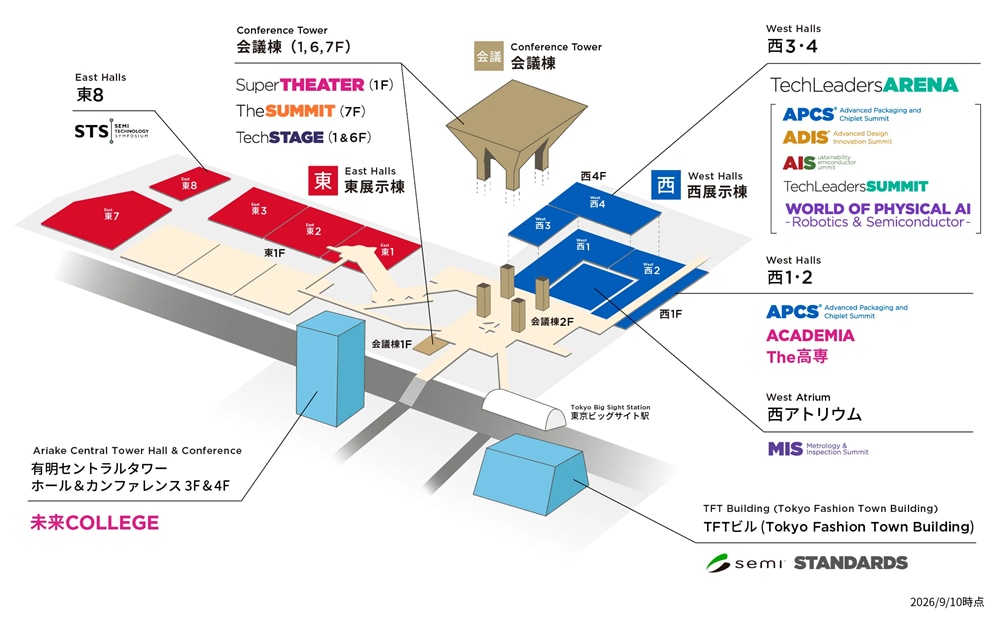
Venue
Tokyo Big Sight
Ariake Central Tower Hall & Conference Tokyo Fashion Town(TFT) Building
Organizer
SEMI
Entrance Fee
Exhibition: Free need to register
Seminars: Some are fee based
Hitachi High-Tech Group Booth
Hitachi High-Tech Group Booth
(Exhibition Products)
Our company leverages four core technologies, Processing, Observation, Measurement, and Analysis, to provide mission-critical tools and digital solutions that support semiconductor manufacturing from R&D to high-volume production. By harnessing diverse digital data, AI, and O&M domain expertise, we deliver HMAX™ Industry for Semiconductors, optimizing operations across the entire Lab-to-Fab journey. At this exhibition, we will showcase world-class solutions that integrate our four core technologies with digital capabilities, helping maximize value across the entire semiconductor manufacturing value chain.
We will also feature a sustainability exhibit. Stage shows featuring HMAX™ Industry for Semiconductors and a Happy Hour will be also held at our booth. For more details, please see the Hitachi High-Tech Group Booth (Events).

- Conductor Etch System M-600 Series
- Conductor Etch System 9000 Series / 9060 Series
- Dry Etching System GAEA-series
- Plasma Treatment System NEMST-D2002ILD
- Formic Acid Reduction Vacuum Reflow System MPW / MPX1
- Wet Processing System ETS-series
- Laser Annealing System LAPOLLON, Laser De-Bonding System WD400U
- Compact Multi-Function Edge Grinding System for Glass Substrates NMPG-450
- CMP System for PLP Substrates LS500
- [Special corner]Smart Maintenance demonstration by VR technology
- Multi-View Defect Observation SEM
- Dark Field Wafer Defect Inspection System DI2800
- Mirror Electron Inspection System Mirelis VM1000 (Reference exhibit)
- Wafer Surface Inspection System LS9600 /
Dark Field Wafer Defect Inspection System DI4600 - Defect Review SEM CR7300
- Scanning Acoustic Tomography (SAT) WAFER LINE
- X-ray Inspection System TUX-8000, MUX-3500, MUX-2021
- High-Precision Electron Beam Metrology System GT2000
- Advanced CD Measurement SEM CG7300
- High Voltage CD-SEM CV7300
- Hitachi High Resolution FEB CD Measurement SEM CS5000
- System Solution of CD-SEM
- Offline Recipe Creation system RecipeDirector /
Offline Multi-Function Measurement system DesignGauge-Analyzer Plus /
Online High-Speed Multi-Parameter Measurement System MI-Boost - X-ray Fluorescence (XRF) Coating Thickness Measurement System FT160
- TGV Inspection System 3D NIR Tomography, TSV Inspection System Via Master A300
- 【Special corner】
BEYOND MEASUREMENT
Shaping the Future of Fabs with Physical × Intelligence
Hitachi High-Tech System Solutions
- Sustainable Solution
- Semiconductor analysis using TEM / SEM technologies
- Ultra-high Resolution Scanning Electron Microscope SU9600
- High Resolution FE-SEM SU8600 / SU8700
- SEM based dedicated nano-probing system NP8000
- High Resolution Schottky Sccaning Electron Microscope SU3900 / SU3800 SE Series
- Ion Milling System IM4000II / ArBlade 5000
- Hihg Performance FIB-SEM NX5000 series
- Quality Issue Management System
Hitachi High-Tech Group Booth (Events)
The following events will be held at the Hitachi High-Tech Group booth. We look forward to welcoming you.
1. HMAX Industry for Semiconductors Stage Show
Dec. 9th/11th: ①10:30 ②11:30 ③12:30 ④13:30 ⑤14:30 ⑥15:30 ⑦16:30
Dec. 10th: ①10:15 ②11:00 ③11:45 ④13:00 ⑤13:45 ⑥14:30 ⑦15:30
2. Happy Hour
Dec. 10th: 16:00~17:00

Exhibitor seminar (Free)

Date
13:30~14:20 on Dec. 10th
Venue
West Hall2 Meeting Room (2) (Private Space),
Tokyo Big Sight
(EXHIBITOR'S TechSPOT)
Theme
Hitachi Inspection & SEM Review Solutions Introduction and Technical Consulting Seminar
In this seminar, we will introduce estimation examples and practical approaches for loss cost reduction.
The session will conclude with an open consultation forum, where participants can discuss their day-to-day challenges and questions with our experts.
Others
For the details, please check the Web page of SEMICON Japan 2026.