- Review SEM Featuring Double Defect Imaging Speed –
FOR IMMEDIATE RELEASE
Tokyo, November 26, 2020 – Hitachi High-Tech Corporation (President and CEO: Masahiro Miyazaki / Hitachi High-Tech) announced today the launch of the high-speed defect review SEM*1 CR7300. The CR7300 is a new model of review SEM that will contribute to the productivity improvement in the manufacturing of cutting-edge semiconductor devices. Enhanced electron optics allows to acquire best high-resolution images to date, while advanced imaging and stage systems are enabling high speed image acquisition in half of the time compared to conventional methods greatly reducing total inspection time.
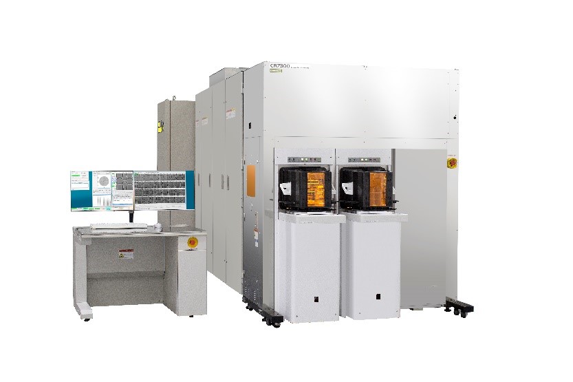
【High-Speed Defect Review SEM CR7300】
As major logic device manufacturers are beginning to develop 3nm generation devices, and starting mass production of 5nm generation devices utilizing advanced process technologies, the miniaturization of device structures requires to acquire and analyze more images of microscopic defects at high capture rates and short turnaround time. The memory device manufacturers are developing vertically layered multiple-memory-cell structures (3D-NAND), which are being introduced to Flash-Memory. Therefore, it is required to perform defect review of high aspect ratio trenches and holes with higher sensitivity. Moreover, there is an increasing demand for electrical characterization*2 to be carried out during the manufacturing process. To help high end device manufacturers to fulfill these requirements, CR7300 has the following features:
The newly developed electron optical system and high-speed imaging system enable fast beam scan at twice the speed of conventional methods, while an enhanced wafer transfer system reduces wafer loading times. As a result, the total performance of defect imaging per hour is approximately twice as fast as previous tool models. Automatic defect review (ADR) performance with enhanced imaging technologies is able to contribute to the productivity improvement in the manufacturing of cutting-edge semiconductor devices. New EDS*3 (elemental analysis) system that utilizes high sensitivity X-ray detectors, is enabling elemental analysis of defects in less time than ever before.
The newly developed VT-Scan*4 enables visualization of electrical characteristics of memory devices, and it is able to detect electrical defects during the early manufacturing process.
New electron optics enables high resolution imaging of microscopic defects and provides advanced image processing using artificial intelligence (AI) to further enhance the image quality. In addition, it features newly developed dark-field optical microscope for non-patterned wafer review function. It allows to improve capture rates for microscopic defects on the none-patterned wafers required for advanced process development.
Hitachi High-Tech has made effort to meet customers’ needs in metrology and inspection for the R&D and mass production of semiconductor market by supplying electron beam based products such as traditional CD-SEM and wafer inspection systems based on optical technologies. Hitachi High-Tech will continue to provide innovative solutions for upcoming technology challenges. Furthermore, Hitachi High-Tech will contribute to the development of cutting-edge technologies by pursuing and creating new value in collaboration with its customers.
| Model | CR7300 |
|---|---|
| Wafer Size | ø300 mm (SEMI standard V-notched wafer) |
| Auto-loader | Random access compatible with 2FOUP*5 |
| Power Supply | Single-phase 200 VAC, 208 V, 12 kVA (50/60 Hz) |
Arai
Nishikawa
