Helping to ensure quality and reliability of semiconductor devices in the IoT and automotive fields
FOR IMMEDIATE RELEASE
Tokyo, November 27, 2020 – Hitachi High-Tech Corporation (President and CEO: Masahiro Miyazaki / Hitachi High-Tech) announced today the launch of the 3D SEM*1 CT1000, that is required for defect observation in the semiconductor industry. This product enables 3D observation of pattern and defects shapes that occur during the manufacturing process on wafers up to 8 inches (200 mm) in diameter, with a feature to analyze the elemental composition of objects being observed. This product will help to contribute to the quality assurance on IoT (Internet of Things) and in-vehicle automotive semiconductor devices.
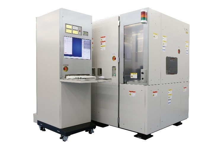
【3D SEM CT1000】
In recent years, with the rise of electric vehicles and smartphones using 5G network, the IoT and in-vehicle device market has seen an increase in the number of IC chips being installed, and a consequent demand for higher-quality, safer, and more reliable three-dimensional structured semiconductor devices. Following this trend, Hitachi High-Tech has been actively engaged in development of inline shape observation SEM products that allow users to check the structure of three-dimensional devices on a wafer during manufacturing process and observe any defects that may have occurred during pattern formation.
Hitachi High-Tech launched the CS4800 high-resolution FEB*2 CD-SEM for the IoT and in-vehicle automotive markets in 2015, which helped to increase productivity by meeting customers’ demand for high-precision pattern dimension measurement in these fields. In addition to this CD-SEM, we are launching the CT1000 to meet the demands for defect inspection and pattern shape observation on existing lines within these markets.
The CT1000 can automatically transport wafers of up to 8 inches (200 mm) in diameter and accurately move to the pattern location to be observed for defects. The sample stage can be tilted to perform 3D SEM observation. If a defect is found, it can perform elemental analysis of the relevant defect. Elemental analysis can be used to analyze factors causing yield decrease and can help to improve the quality of semiconductor devices in development and manufacturing processes. After reviewing defects and pattern shapes, the wafer can be returned to the manufacturing line, improving manufacturing process efficiency.
A unique feature of the CT1000 is the ability to observe 3D SEM images using the sample stage tilt function. To achieve this capability, Hitachi High-Tech has developed a conical objective lens that allows wafers to be tilted up to 55°. The five-axis sample stage was developed to prevent significant movement of the center of a wafer when observed from directly above, even if the sample stage is tilted to the maximum inclination angle. This makes it possible to better capture target defects and increase work efficiency.
Hitachi High-Tech has made effort to meet customers’ needs in metrology and inspection for the R&D and mass production of semiconductor market by supplying electron beam based products such as traditional CD-SEM and wafer inspection systems based on optical technologies. Hitachi High-Tech will continue to provide innovative solutions for upcoming technology challenges. Furthermore, Hitachi High-Tech will contribute to the development of cutting-edge technologies by pursuing and creating new value in collaboration with its customers.
| Model | CT1000 |
|---|---|
| Resolution | 7nm@1kV |
| Maximum sample tilt angle | 55゜ |
| Size of observation field | 0.675 to 135 µm |
| Elemental analysis (optional) | Energy-dispersive X-ray spectrometer |
| Measurable wafer size | SEMI standard 200-mm Si wafer |
Sakai
Nishikawa
