
What is Silicon Photonics?
Silicon photonics is a technology for fabricating optical and electronic integrated circuit on silicon microchip. Since the 2000s, research and development has been carried out at major corporate research institutes. In recent years, silicon photonics have attracted attention because the development of communication technology has increased the demand for fast and efficient transmission and reception of data. And some companies, with recent research, have finally moved into the commercialization phase and started to provide and manufacture silicon photonics products. In this article, with the cooperation of VLC Photonics S.L., which designs and proposes photonic integrated circuit and provides services utilizing its network with a wide range of foundries, we introduce the basics and business cases of silicon photonics.
Silicon photonics is a technology that integrates elements such as photodetectors on a silicon substrate.
Silicon photonics is a technology that integrates elements such as optical waveguides, optical switches, optical modulators, and photodetectors on a silicon substrate. In recent years, as the amount of information distributed has increased, the information and communication technologies that support it are required to be able to handle faster processing, a huge economic burden, and energy consumption. Silicon photonics has attracted attention because of its economic efficiency, high integration density, and high energy efficiency. In recent years, silicon photonics has been used in communications and sensors, and is expected to be applied to the development and spread of IoT and 5G.
Characteristics of Silicon Photonics
- High-speed transmission
- Smaller devices and lower power consumption reduce environmental load
- Can be manufactured relatively inexpensive by using the silicon CMOS integrated circuit manufacturing infrastructure
Differences between photonic integrated circuits such as silicon photonics and optical units
What makes a photonic integrated circuit different from the same optical technology? Let’s compare this to an optical unit that combines multiple optical elements.
Photonic integrated circuits can be smaller than optical units
In an optical unit, individual optical elements are fixed to the housings, arranged and assembled, while a photonic integrated circuit can be integrated on one chip, making it smaller.
Photonic integrated circuits can operate with less light energy than optical units
Compared to optical unit that operates between optical elements arranged on a housing, photonic integrated circuit can operate with minute light energy because of its structure combining integrated micro optical elements. In addition, it takes advantage of the strong optical confinement effect of the photonic crystal structure, which miniaturizes the device and requires less optical energy.
Three examples of R&D and practical application of silicon photonics
Today, around the world, there are efforts to R&D and commercialize silicon photonics.
1. Modulator downsized to 1/1000 / Intel
At “Intel Labs Day 2020” in December 2020, silicon photonics was a research topic to focus on. A modulator that was reduced from the conventional component size to 1/1000 of it was introduced.
2. Developed optical transmission module using silicon photonics / NTT
To realize all-photonics network that introduces photonics-based technologies into everything from networks to terminals, NTT developed optical transmission module using silicon photonics.
3. Work with foundries to propose flexible solutions / VLC Photonics
VLC Photonics (hereafter called “VLC”), in Valencia, Spain, supports the development of photonic integrated circuits including silicon photonics and designs LiDAR (Light Detection and Ranging, a light-based remote sensing technology) for optical communication and self-driving cars, and silicon photonics for fiber sensos. As a fabless company, through its extensive networks of chip foundries, VLC proposes the best solutions for products and applications.
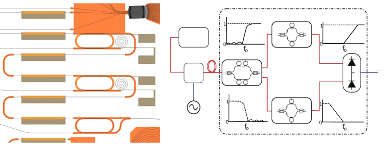
Six steps for fabricating photonic integrated circuit by silicon photonics
Silicon photonics is currently attracting attention in the fields of optical communication, sensing, and bio-photonics. Let's look at the process of designing and manufacturing a photonic integrated circuit using silicon photonics.
- Compatibility Survey Investigate and examine the appropriateness of photonic integrated circuit creation for applications and businesses
- Engineering Study Based on the specifications of optical systems, VLC examines the specifications required for photonic integrated circuits.
- PIC Design Design optical components and circuit layout
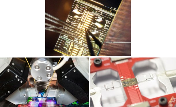
- Fabrication Manufacture VLC designed PIC at foundry
- Characterization Evaluate the characteristics of the photonic integrated circuit and test whether its performance meets the requirements. Then, VLC examine the assembled version as the system level.
- Packaging Package photonic integrated circuit and other components together
Process flow of design and fabrication of Integrated Optical Circuit.
Completion of photonic integrated circuit requires specialized knowledge and know-how in each of the design, test, and production phases. However, VLC can provide consistent support from prototype development to mass production.
Silicon Photonics expected for applications in communications, automotive, medical and other fields.
Silicon photonics is expected to be used in a variety of fields, not just telecommunications. In Japan, in the automotive field, research make progress toward the practical application of silicon photonics for LiDAR, which is essential for autonomous driving. In the field of quantum communications, experiments using silicon photonics and photonic integrated circuits are being conducted and studied at universities and research institutes. VLC can support you from the research stage to the manufacturing stage. In addition, the application of photonic integrated circuit technology is expected in the field of bio-photonics, which is attracting even more attention these days. VLC is participated in PIX4life, an open platform for the introduction of photonic integrated circuit technology in the life sciences field in Europe, and also embarks on an initiative to introduce optical integrated circuit technology in the medical field. Silicon photonics is expected to be further developed and applied in the future. If you are interested in photonic integrated circuits or are looking for a partner with solid knowledge and know-how, why not consult VLC?
About VLC, the company that helped write this article.
Totally support customers' realization of photonic integrated circuits in both business and technical perspectives.
Spun out of the Technical University of Valencia, Spain, VLC is a fabless company that designs silicon photonics and other photonic integrated circuits. In 2011, VLC was founded by Jose Capmany, a professor at the university, and Pasqual Muñoz, an associate professor at the university. The members have high level academic knowledges, and they help customers to create photonic integrated circuits.
Support from the business side as well as the technical side
VLC understands the information of various industry trends and their standards, and they are possible to evaluate the required specifications and the cost of photonic integrated circuits. Moreover, they can estimate the price from R&D to the mass production stage, which enables us to evaluate and examine both business and technology aspects.
Photonic integrated circuit can be designed using not only silicon but also other compound semiconductors.
In addition to designing with silicon photonics, VLC is also good at designing with other compound semiconductors such as InP (indium phosphorus) and GaAs (gallium arsenide). In the future, photonic integration technology is expected to be applied to all kinds of applications, but in some cases, silicon may not meet the requirements. Usually, it is said that other companies that design photonic integrated circuits often specify silicon as the material to be used, for example, but at VLC, the members have research experience and deep knowledge about not only about silicon but also various semiconductor compounds, so they can present a wide range of solutions and better meet customer needs.
Can also be tested after fabrication of photonic integrated circuits.
It is said that most other fabless companies do only design, but VLC can evaluate the performance of PIC after design and manufacture. After the fabrication, the properties of the circuit are tested, and if it does not meet the requirements, improvement measures are proposed to consistently support prototyping from design, manufacturing and packaging. VLC has semiconductors to drive the chips, measurement components such as optical probes, and test equipments, so when a customer requests a test, they can respond immediately. In addition, VLC has equipment that can be tested not only at the chip level but also at the wafer level, greatly reducing inspection time. One of the challenges for practicalize and mass-production of silicon photonics is that there is a large gap between the simulation results at design time and the performance after actual packaging. VLC is committed to solving this problem by accumulating in-house expertise in characterization and data on evaluation results.
Have wide foundries network
While VLC designs photonic integrated circuits made of a variety of silicon series and compounds, they are good at selecting foundries and collaborating with them according to their base materials. In the packaging of PIC, they also have partnerships with various packaging companies, so they can provide packaging services that meet customer needs. Even if they can design photonic integrated circuit, we need to consider manufacturing issues such as whether it can be manufactured and what the yield is. Through cooperation with many foundries, VLC has accumulated know-how that enables it to design products with higher yields based on product and foundry characteristics. Therefore, VLC can select and propose the best foundry for the customer's desired design.
Internationally recognized Technological capabilities
VLC's technological capabilities are internationally recognized. In 2019, they were awarded the "Best Achievement In PIC Development," which is awarded to the company that has performed the best in the design of photonic integrated circuits. In the same year, they were awarded the "Lightwave innovation award" in recognition of its work not only in the field of PIC but also in that of optical communications. They also participate in a number of R&D projects in Europe. For example, when they participated in an international project called “CiViQ” to build platform for quantum communication in Europe, they designed photonic integrated circuit inside a communication module with advanced security.