
Yasuo Katakura
Masahiko Tsujita
Noriyoshi Yamauchi
Toshio Kawamura
Sony Semiconductor Manufacturing Corporation
It is important to analyze and investigate defective products during semiconductor manufacturing processes in the early development stage, in order to improve the final yield and quality. Therefore, in a failure analysis department, it is necessary to be able to identify defects that can lead to device failure with a high success rate. The success rate in identifying defects that can lead to short circuits in wiring or to gate leaks tends to be low for CMOS image sensors. Therefore, we developed a new analysis technique that can diagnose defects in microscopic regions, with a resolution much higher than that for current techniques. We focused on dynamic induced electron-beam absorbed current (DIEBAC), which it is based on the EBAC method, but allows the application of a bias voltage during the analysis. Herein we report the results of an analysis of a CMOS image sensor using the proposed technique.
The ongoing trends of miniaturization and multilayering in fabrication processes for CMOS image sensors have increased the prevalence of various types of defects, including both short defects—such as gate leaks and accidental junctions between interconnect lines—and open defects such as ruptures in interconnect lines. Of these, the former is significantly more difficult to diagnose: the causes of short defects are correctly determined at around 20% lower rates than those of open defects. This discrepancy is due to the characteristic structure of CMOS image sensors, as illustrated in Figure 1: for open defects, the address of the defect is readily identified from the image, but short defects cause all pixels within the same node to be displayed in the image, leaving the defect address ambiguous.
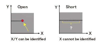
Fig. 1 Open/Short defect image on CMOS image sensor
At present, the primary strategies for detecting short defects are analytical methods using optical or laser light, such as lock-in thermal detection or infrared optical beam induced resistance change (IR-OBIRCH). Although these are powerful techniques capable of locating microscopic defect regions within broad sample areas spanning entire devices, their spatial resolution is limited. This is illustrated in Figure 2, which shows the results of (a) L-thermal and (b) IROBIRCH analyses of short defects in the interconnect wiring of CMOS image sensors. As is evident from these images, the accuracy with which these methods are capable of locating defects ranges from hundreds of microns to—at best— a few microns. Pinpointing defect sites with greater precision requires wide-area delayering and in-plane observations, which tend to reduce the likelihood of successfully determining defect causes. Thus the development of new methods for analyzing short defects is an increasingly urgent priority.
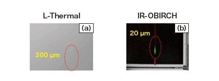
Fig. 2 Image of current optical analysis method
The first point to consider is how to achieve high spatial resolution. For this we must take into account the spreading of beams due to diffractive aberration. From basic Rayleigh optical theory, the resolution is related to the wavelength by Eq. (1) in Figure 3. By using incident light with shorter wavelengths we can reduce diffractive aberration and improve spatial resolution. Thus, in addition to optical and laser sources mounted on the analytical instrument, we consider the wavelength of the electron beam. Note that, as is clear from Eq. (1), the resolution may also be improved by increasing the aperture angle Θ; however, for electron beams it is not possible to achieve strictly zero objective-lens aberration, and this places practical limits on the maximum attainable resolution. This is illustrated in Figure 4. For a transmission electron microscope (TEM), the resolution is determined from the spherical aberration coefficient and the wavelength by Eq. (2); here again we see the importance of selecting irradiating light of short wavelength.
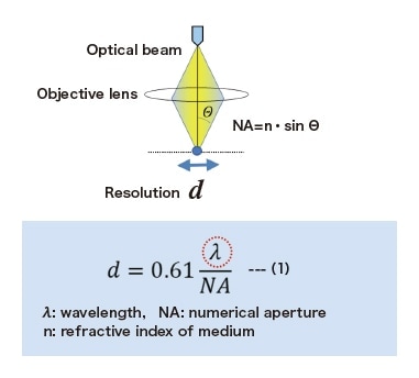
Fig. 3 Resolution of optical beam
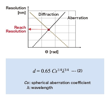
Fig. 4 Resolution of transmission electron microscope
The wavelengths of optical and electron beams are given by Eqs. (3) and (4) respectively. The variable in Eq. (3) is the frequency of the light, while Eq. (4) is an approximation in which the variable is the accelerating voltage of the electron beam.
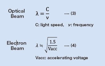
Figure 5 plots the electron-beam wavelength versus the accelerating voltage [Eq. (4)] over the range 5-30 kV used in scanning electron microscopy (SEM). In this range the wavelength varies from 0.2 to 0.5 nm, an enormous reduction compared to the near-infrared light wavelengths used for thermal detection or IR-OBIRCH. We next investigate the improved resolution enabled by the use of electron-beam techniques.
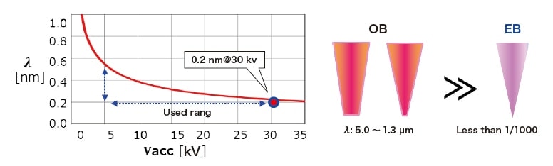
Fig. 5 Comparison between optical beam and electron beam
One well-known electron-beam technique is electron beam absorbed current (EBAC) using a nano-probe, in which currents absorbed by metal interconnects are detected while an electron beam is scanned over a sample. In this approach, equipotential pathways are highlighted, yielding a powerful tool for detecting open defects such as ruptures in interconnect lines. It is also possible to detect electron-beam induced current (EBIC) resulting from the creation of electron-hole pairs by electron-beam irradiation of a silicon substrate.
Figure 6 shows a schematic depiction of the EBAC approach and images from EBAC studies.
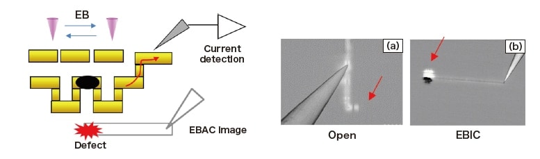
Fig. 6 EBAC overview and image
One drawback of EBAC is that, as a technique for visualizing equipotential pathways, its ability to pinpoint short defects is limited. This is illustrated in Figure 7, which shows EBAC images of short defects in an interconnect layer (c) and a Tr layer (d). In both cases, the EBAC analysis indicates the entire short-circuit pathway, failing to identify the location of the defect.
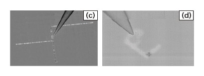
Fig. 7 Short analysis image by EBAC
Figure 8 graphically depicts the spatial resolution and resistance sensitivity of experimental methods available today. Our target in this work is the upper-right region of this graph, in which resistance defects can be located with submicron precision.
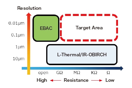
Fig. 8 Resolution and Defect resistance value
As a remedy for the difficulties discussed above, we focus on dynamic induced EBAC (DI-EBAC), a form of EBAC allowing the application of biases. Our rationale for this choice is that the application of biases allows short defects to be reproduced with high certainty, while EBAC analysis of reproduced configurations allows changes in the state of defect sites to be accurately detected in the form of current variations.
Figure 9 illustrates the principles of DI-EBAC, which augments conventional EBAC by adding a means of applying biases. In this approach, the electron beam is scanned over a sample—as in conventional EBAC—but now with a bias applied to pathways believed to contain defects.
The basis of the method is the local temperature increase induced in electron-beam irradiated sample regions, given by Eq. (5) according to Castaing’s theory. The variation in temperature induces changes in the thermoelectromotive force and thermal resistance at defect sites, yielding current variations which are amplified and detected.
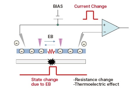
Fig. 9 Principle of DI-EBAC
![θ m[℃ ] = 477*I*V/(C*d)](/image/global/sinews/si_report/130214/index_12.jpg)
In testing the efficacy of DI-EBAC, we focus on three items in particular:
Of these, the resolution [point (1)] is determined by the convergence of the electron beam, as discussed in Section 2-1; the ability to constrict electron-beam wavelengths to below 1 nm promises higher resolution than can be achieved via optical methods. Our goal is to localize defect sites within regions small enough for cross-sectional analysis via scanning transmission electron microscopy (STEM), i.e., to within 0.2 μm.
Regarding transparency [point (2)], Figure 10 shows a schematic depiction of EBAC and the pattern of electronbeam spreading. In order to detect the defect shown in the figure, the electron beam must pass through the upper layer to reach the defect site. The penetration properties of electron beams are determined by the accelerating voltage and the atomic density of the material, which we have studied via Monte-Carlo simulations as shown in the figure. We see that, for an accelerating voltage of 30 kV, the beam penetrates bulk Cu to depths of up to several microns, and as CMOS image sensors contain 3-5 interconnect layers, this should suffice to assure access to even the lowest layers.
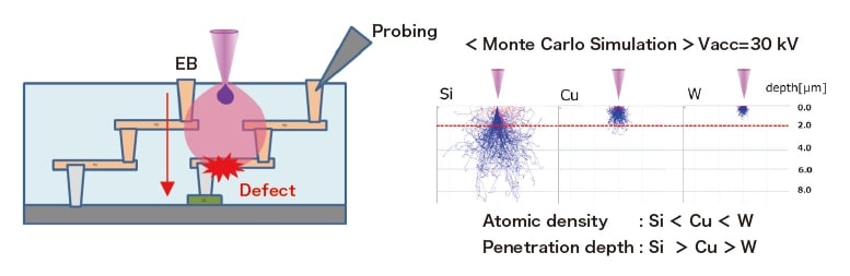
Fig. 10 Electron beam transmission characteristics
Finally, regarding the effect of applied bias [point (3)], we note that, because EBAC images are produced by electronbeam irradiation, applied currents constitute a type of noise that may impact the sensitivity of the analysis.
The importance of choosing parameter settings to ensure that applied currents do not affect the sensitivity is a significant difference between this method and OBIRCH, in which the irradiating light source is a laser.
In view of the above considerations, we next validate our method experimentally.
Figure 11 shows the results of a test involving a gate defect. For two samples (S1 and S2) believed to contain damaged gates, we expose the gate and source contacts and apply probes and biases. In images (a) and (c), obtained via conventional EBAC analysis, the entire component region is visible, preventing clear identification of defect sites. In contrast, the DI-EBAC images (b) and (d) reveal localized response regions with sizes of 0.10 - 0.15 μm.
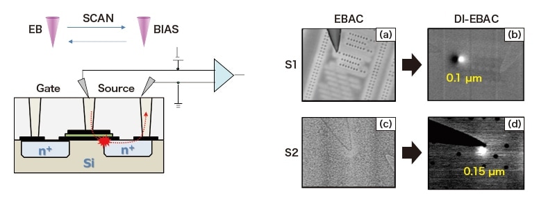
Fig. 11 DI-EBAC result for gate leak defect
Figure 12 shows the results of a cross-sectional analysis of the S1 sample region near the DI-EBAC reaction site. In the STEM image (f), a short defect is seen between the W contact and the Si substrate. Electron-beam irradiation of short-circuit pathways between different materials produces a thermoelectromotive force via the Seebeck effect, which is detected through variations in current. This example demonstrates that, as expected, DI-EBAC offers high resolution and is a powerful tool for short defect analysis.
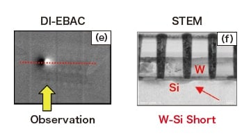
Fig. 12 Cross-sectional image of reaction part
We next validate our method by detecting short defects between adjacent interconnect lines. As shown in Figure 13, we expose and apply probes to the sample layer believed to contain defects. The exposed region opens a portion of the chip edge to avoid losing the defect. The DI-EBAC image (a) shows that the defect is detected in the fourthdeepest layer. In this region, defect scanning of the production line reveals an irregular formation spanning multiple interconnect lines [image (b)]. Image (c) shows EBIC reactions not of defects but of Tr connected to probing pathways. This observation of charge transport from the Si substrate further demonstrates the ability of our analytical technique to bypass upper interconnect layers in detecting defects on lower layers.
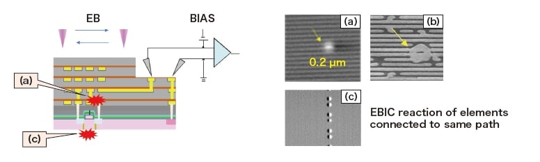
Fig. 13 DI-EABC result for metal short defect
Figure 14 shows results of similar measurements of interconnect defects of varying resistance values. The resistance of the samples decreases from image (d) to image (f), but reactions are clearly visible in all cases. In particular, the successful result in the case of image (f), which at 70 Ω was the lowest resistance of all defects we considered, demonstrates that the sensitivity of DI-EBAC extends over a broad range of conditions ranging from high to low resistance.
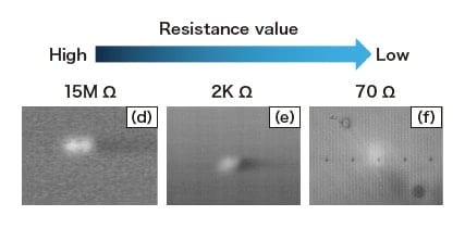
Fig. 14 DI-EBAC Image by defect resistance value
We next investigate the interaction between electron-beam sample irradiation and applied bias. In selecting the electron-beam irradiation conditions, we note that stronger beams offer more energy to activate defects, and thus we set the beam current to its maximum value of 30 μA, for which the actual beam current impinging on the sample surface is 29 nA. Keeping this condition fixed, we then acquire DI-EBAC data while varying the applied current bias. The results are shown in Figure 15. For zero applied current, there is no response; a response begins to appear at an applied current near 0.1 nA [image (a)], and the response is clearest at an applied current of 1 nA [image (b)]. Further increasing the applied current decreases the intensity of the response [images (c), (d)], and at 1 μA there is almost no response. This is illustrated in Figure 16, in which we plot the relative brightness of the response site versus the applied current. The relative brightness is the difference in brightness between the response site and its vicinity, taking into account the displacement of electric charge on the sample surface. The results indicate that the relative brightness is high when the applied current is less than the irradiating electron-beam current, and decreases for larger applied currents. We attribute this to reduced sensitivity due to a reduction of the signal-to-noise ratio, as the applied current constitutes a type of noise. On the other hand, for applied currents much larger than the electron-beam current, on the order of hundreds of μA, the current-flow pathways themselves are highlighted, as in image (f). We interpret this as follows: large applied currents create magnetic fields that deflect the irradiating electron beam, causing it to be detected by the probe; thus, as the magnitude of the applied current increases, there is a change from a localized response at the defect site to the entire current-flow pathway.
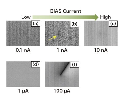
Fig. 15 DI-EBAC Image by applied current
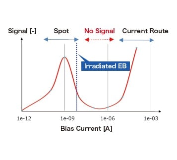
Fig. 16 EBAC Signal and Applied current
These findings show the importance of tuning the applied bias appropriately for a given irradiating electron beam. In Figure 17 we superpose DI-EBAC and SEM images of a sample region for two different applied-current values. At an applied current of 1 nA [image (h)] we obtain a response localized at a defect site, while for 100 μA [image (i)] the entire current-flow pathway responds. The ability to acquire two types of data simply by varying the applied current yields extremely useful information for pinpointing the location of defects.
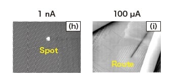
Fig. 17 Difference in reaction mode depending on applied current
The results of our experimental tests demonstrate that DI-EBAC is a powerful technique for analyzing CMOS image sensors, whose advantages include the following:
A key point is the importance of tuning current settings in accordance with experimental conditions, as the detection sensitivity is affected by the applied current. When used together with existing methods, the advantages of our new technique—particularly the use of an applied current to enable accurate defect reproduction and the use of electron-beam stimulation to achieve high resolution and detect low-layer defects beneath multiple interconnect layers—promises the possibility of designing analytical environments capable of seamlessly covering a broad range of situations from open-circuit to short defects.
References
About the Authors
Yasuo Katakura, Masahiko Tsujita, Noriyoshi Yamauchi, Toshio Kawamura
Sony Semiconductor Manufacturing Corporation
See more
