
Shigeto Yamasaki
Ph.D (Engineering)
Associate Professor
Department of Materials
Kyushu University
Observations of dislocations are of crucial importance for structural analysis of crystalline materials. Figure 1 shows a scanning electron microscopy (SEM) image of dislocations in silicon obtained via electron channeling contrast imaging (ECCI). In recent years, it has become possible to capture SEM images of dislocations with a clarity rivaling that of TEM images. However, most research studies reporting ECCI observations of dislocations have not carefully optimized the electron-beam irradiation conditions, and in many cases the analysis of dislocation substructures has been limited to semi-quantitative treatments. For accurate characterization of dislocation motion and dislocation densities, it is essential to use g·b analysis to determine Burgers vectors and to clarify the visibility or non-visibility of dislocations under the conditions of a given observation. Also, the incidence direction of the electron beam (e-beam) must be accurately determined when estimating e-beam penetration depths (extinction distance) in ECCI images. Only when detailed information of this nature is available can ECCI observations of dislocationstructures replicate the quality of TEM observations1) .
Techniques for determining the e-beam incidence direction in SEM include the electron channeling pattern (ECP) and selected-area electron channeling pattern (SACP) methods, as well as the electron back-scattered diffraction (EBSD) method. Historically, the field evolved from the ECP and SACP methods to the EBSD method to allow higher-speed crystal orientation mapping. Thus, the development of EBSD temporarily rendered ECP and SACP obsolete. However, more recently, these methods have returned to the spotlight due to the need for high-precision determination of the e-beam incidence direction in quantitative ECCI observations. In this paper we present several illustrative examples of SACP-enhanced ECCI observations performed using an SEM system equipped with an e-beam tilt controller.
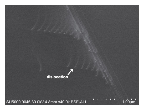
Fig. 1 Dislocations in silicon observed via SEM-ECCI.
As noted above, EBSD is the most commonly-used method for determining the e-beam incidence direction in SEM. However, the use of EBSD to measure the crystal orientation requires that the sample be tilted at an angle of approximately 70°, which is problematic because when this is used to infer the e-beam incidence direction in the non-tilted state, errors as large as 2° have been reported to arise2). When determining an e-beam incidence direction appropriate for use in ECCI observations, errors of this size are fatal, and thus conducting quantitative ECCI observations based on EBSD orientation data—while not strictly impossible—is extremely difficult.
This motivates consideration of ECP and SACP as alternatives to EBSD for determining the e-beam incidence direction. Figure 2(a) shows a backscattered-electron (BSE) image of single crystalline silicon, acquired at low magnification (×50). Despite the single crystalline nature of the sample, a geometric pattern is visible on the sample surface; this is known as the electron channeling pattern (ECP). When observing low-magnification SEM images, the angle between the incident beam and the sample surface varies significantly depending on the e-beam scan position, as illustrated by the schematic depiction of e-beam irradiation shown in Figure 3(a). Whenever the incidence direction of the e-beam happens to satisfy the Bragg condition, the BSE intensity becomes weak, and thus BSE images show a characteristic pattern reflecting variations in the e-beam incidence direction; this is the ECP3). Because the ECP reflects the crystal orientation of the sample, it can be analyzed to determine the incidence direction of the e-beam. Alternatively, fixing the e-beam irradiation point and varying the tilt angle of the irradiating e-beam (known as beam locking) yields a similar pattern known as a selected-area electron channeling pattern (SACP), as shown in Figure 3(b). Figure 2(b) shows an SACP acquired at the same sample position as in Figure 2(a). As these images demonstrate, SACP images acquired with the use of an e-beam tilt controller reveal patterns similar to those in ECP images, but with greater clarity and sharpness, and thus the SACP approach can determine the e-beam incidence direction more accurately than the ECP approach.
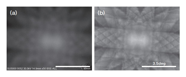
Fig. 2 (a) BSE image of single crystalline Si sample acquired at low magnification. (b) SACP acquired for same sample.
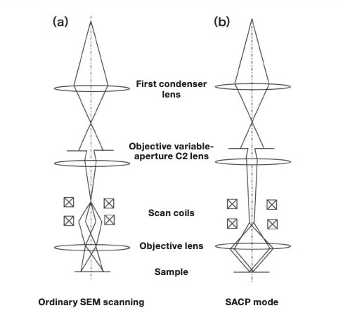
Fig. 3 Schematic diagrams illustrating e-beam irradiation configurations for (a) ordinary SEM scanning, (b) SACP acquisition. Source: Taken from the instruction manual for the SU5000 e-beam tilt controller.
Among the most important advantages of SACP over ECP is its greater spatial resolution. As is clear from Figure 2(a), ensuring an adequate range of e-beam tilt angles for ECP images requires large fields of view, on the order of millimeters; thus, in practice, the ECP approach to incidence direction determination is only applicable to single crystalline samples or samples with very large crystal grains. In contrast, the use of a suitable e-beam tilt controller— such as the e-beam tilt controller installed on the Hitachi SU5000—allows acquisition of SACP images for irradiated regions as small as 5 μm. One complication of the SACP method is that the impact of lens spherical aberration becomes particularly pronounced at high tilt angles. For this reason, modern SEM systems featuring SACP modes are equipped with spherical aberration correction capabilities to allow both high tilt angles and ultra-small irradiation regions. Figure 4 illustrates the process of calibrating such a spherical aberration corrector, in this case using a Cu mesh with a linewidth of approximately 5 μm and a grid spacing of approximately 25 μm. When calibration is in progress [Figure 4(a)], several mesh lines are visible in the field of view, and the irradiated region extends over a wide area of approximately 200 μm. Also, different numbers of mesh lines are visible in the upper and lower portions of the field of view, indicating that the region is not irradiated isotropically. After calibration [Figure 4(b)], the intersection of mesh lines extends over the entire field of view, and the size of the irradiated region is reduced to just 5 μm.
This example demonstrates that the SACP approach, applied to individual crystal grains in polycrystalline samples, is capable of determining the e-beam incidence direction with high precision, on the order of 0.1° 4). In such a measurement, the ability to switch back and forth between ECCI and SACP observation modes with just the touch of a button—and with no need to modify the sample tilt angle or any other observation conditions—is extraordinarily valuable. To draw an analogy to standard TEM practices, this approach to ECCI observation is reminiscent of the ability to alternate between acquiring TEM images and diffraction patterns while adjusting observational conditions and searching for target fields of view.
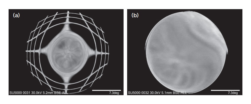
Fig. 4 Calibration of spherical aberration corrector in SACP mode. (a) Calibration in progress. (b) Calibration complete.
Figure 5 presents the results of observations in which each ECCI image acquisition was followed by SACP image acquisition. The sample in this case is a polycrystalline nickel-based alloy. Figures 5(a-c) are ECCI images, while Figures 5(d-f) are SACP images acquired from the irradiation points indicated by crosses in the ECCI images. For the crystal grains located at the positions of the crosses in Figures 5(a) and 5(c), we obtain clear SACP images, with the crystal orientations at the centers of the SACP images corresponding to the e-beam incidence direction in the ECCI images. In contrast, the SACP image in Figure 5(e) was captured in the immediate vicinity of a crystal grain boundary, and shows a superposition of the patterns in Figures 5(d) and 5(f). This example demonstrates that clear SACP images can be obtained at observation points in the interior of relatively large crystal grains. However, SACP images for observation points inside crystal grains smaller than 10 μm or observation points near crystal grain boundaries reflect the influence of multiple neighboring grains, and thus must be interpreted with caution. For similar reasons, SACP images tend to be blurry when deformations have forced a rotation of the crystal orientation inside a grain. For this reason, strategies for reducing the size of the selected area in SACP observations have been pursued in a number of recent studies, which have reported combinations of beam-locking and beam-shifting2,4) or stage-locking5) techniques allowing the selected area to be reduced to sub-micron scales.
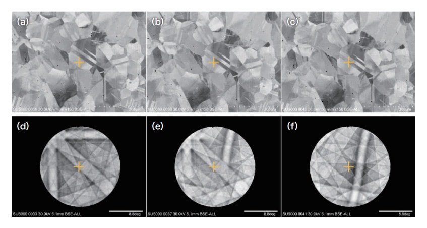
Fig. 5 (a-c): ECCI images of polycrystalline nickel-based alloy sample. (d-f): SACP images acquired for observation points indicated by crosses in ECCI images.
Careful inspection of Figure 5 reveals that the crystal grain contrast at the positions of the crosses in the ECCI images matches the contrast at the positions of the crosses in the SACP images. This is because the contrast in both images reflects the backscattered-electron intensity as determined by the e-beam channeling conditions. For ECCI observations of dislocations, the matching crystal grains are those that satisfy the channeling conditions, i.e., crystal grains that are observed as dark regions in ECCI images. For polycrystalline samples, one approach is simply to find and observe whichever of the many crystal grains in the sample happen to satisfy the channeling conditions. However, the use of SACP enables a more sophisticated observation strategy, in which an arbitrary crystal grain of interest can be observed by tilting the sample until the e-beam incidence direction satisfies the channeling conditions for that grain. In particular, for g·b analysis or other situations requiring a specific incidence direction, the direction of the SACP will be aligned with the target incidence direction, furnishing an extremely valuable roadmap.
In TEM, arbitrary diffraction conditions can be achieved by observing the electron-diffraction pattern while adjusting the inclinations of the α and β axes. Similarly, in ECCI observations, SACP can be used to tilt the sample to achieve arbitrary incidence directions. However, typical SEM stages only offer one adjustable tilt axis. To illustrate how this limitation can be bypassed, we will now present an example demonstrating how a single tilt axis can be combined with stage rotation to tilt samples in arbitrary directions.
The six subpanels in Figure 6 illustrate how the rotation (R) and tilt axis (T) of the stage can be adjusted to ensure that the channeling conditions are satisfied for a specific crystal grain. (The sample here is again a polycrystalline nickel-based alloy). In performing this adjustment we refer to the SACP images shown in the insets of each subpanel. Looking at the orange-outlined crystal grain in Figure 6(a), we see that for R=0° and T=0°, the crystal grain is brightly colored in the image, indicating that the channeling conditions are not satisfied. To ensure that the channeling conditions are satisfied for this grain, we move the dark region within the SACP image to the position of the cross at the center of the pattern. To do this, we adjust the rotation and tilt of the stage until the triangular region indicated in the SACP inset lies at the center of the pattern. First, rotating the stage 35° counter-clockwise yields the configuration in Figure 6(b); in the SACP inset it can be seen that one of the triangles has moved to just below the center of the pattern (at the 6:00 position). Next, from the configuration in Figure 6(b), we gradually increase the sample tilt in the negative direction, yielding the configurations in Figures 6(c-f). As the sample tilt increases, the contrast of the crystal grain evolves, until finally—at a tilt angle of -3.7°—the center of the pattern lies inside the desired triangle [Figure 6(f)] and the crystal grain of interest appears as a dark region in the image, indicating satisfaction of the channeling conditions. Figure 7 is an ECCI dislocation image captured at higher magnification for the sample configuration in Figure 6(f); note that dislocation lines and stacking faults are clearly discernible in this image. This example demonstrates that the use of SACP makes it easy to tilt samples to orientations satisfying channeling conditions, allowing observation of dislocations in arbitrary crystal grains of interest.
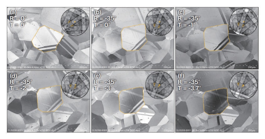
Fig. 6 Adjusting stage rotation and single tilt axis to control e-beam incidence direction.
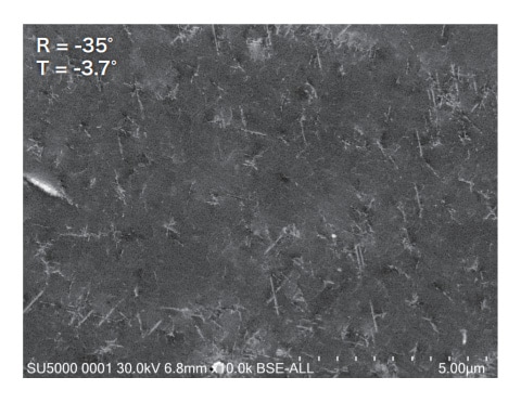
Fig. 7 ECCI image of dislocations captured for configuration in Figure 6(f).
The possibility of using SACP to tilt samples to arbitrary orientations can also be used to determine the Burgers vectors for dislocations via g·b analysis. Figure 8 shows, for a single crystalline sample of BCC iron, ECCI images captured for identical fields of view but for different incidence directions. Note that dislocation lines are clearly discernible in Figure 8(a), but are not observed in Figure 8(b). Using SACP images and Kikuchi pattern simulations to determine the e-beam incidence directions for the two images reveals that the observation conditions in Figure 8(a) result in 20 excitation, while those in Figure 8(b) result in 220 excitation. Because dislocation lines are seen in the first image but not in the second image, the Burgers vector for the dislocations must have a zero inner product with 20 and a nonzero inner product with 20, yielding 4 possible candidates: <11>, <11>, <1>, and <1>. Also, because dislocation lines near the sample surface appear brighter, focusing on one of the observed dislocation lines reveals that the left side is positioned near the sample surface, while the right side lies in the sample interior. In view of these observations, the Burgers vector for the observed dislocations must be either <11> or <1>. This example demonstrates how ECCI observations, in combination with SACP techniques, allow characterization of dislocations in ways that were previously only possible via TEM observations.
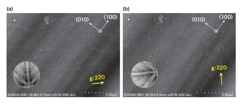
Fig. 8 ECCI dislocation images of same field of view observed for different incidence directions. (a) g=20, (b) g=220.
Before closing we briefly describe one additional purpose for which SACP techniques may soon prove useful: measuring lattice strain. Existing techniques for measuring lattice strain in crystalline samples include X-ray diffraction (XRD) and convergent-beam electron diffraction (CBED), but both of these approaches have limitations. The information obtained from XRD is spatially averaged over the entire bulk sample, while CBED samples are thin films and thus may not accurately reflect the strain properties of bulk materials. An alternative to these approaches is the EBSD method (also known as the Wilkinson method), which can measure lattice strain in submicron-sized regions of bulk materials with dimensions typical of SEM samples. The Wilkinson method measures lattice strain by detecting changes in the widths of Kikuchi bands due to displacements in regions of interest within Kikuchi patterns. If the elastic stiffness for the material is known, this method allows visualization of the stress distribution at each EBSD measurement site.
However, one drawback of the Wilkinson method is the low resolution with which it measures lattice strain. The resolution of typical EBSD cameras—on the order of 1,000×1,000 pixels—can hardly be considered adequate for measuring displacements via image-correlation techniques, and the magnification of pattern images is fixed and cannot be modified. These factors limit the strain resolution of the Wilkinson approach. In contrast, SEM systems can acquire high-resolution images with 5,000 or more pixels per dimension. Moreover, for SACP based on SEM images it is possible to acquire images at increased magnification, as shown in Figure 9. Thus, the ability to acquire SACP images allows the use of longer gauges when using image-correlation methods to measure Kikuchi band displacements, thus promising higher strain resolution. However, as noted above, the selected areas available in present-day SACP methods are rather large—on the order of several microns—and thus high-clarity SACP images cannot be acquired for samples for which the lattice strain varies within the selected area. Thus, successfully using SACP as a tool for lattice-strain analysis may require further improvements in SACP spatial resolution, as discussed in Section 3.
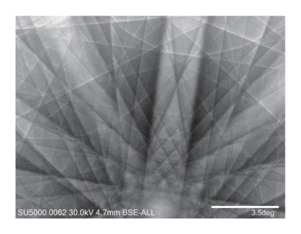
Fig. 9 SACP for silicon sample captured at high magnification.
In this article, we presented several practical case studies demonstrating the usefulness of SACP-based ECCI observations. To exploit the full potential of the ECCI approach to observing dislocation structures, it is important that the various types of quantitative analysis we have discussed be easy to perform. At present, very few SEM systems are equipped with e-beam tilt controllers. However, going forward, we expect it will soon be possible to select specific methods for capturing electron-diffraction patterns for specific applications and objectives—such as the EBSD method for high-speed crystal orientation mapping and the SACP method for high-precision pattern acquisition and control of the e-beam incidence direction—thus enabling further advances in SEM techniques for structural analysis of crystalline materials.
References
See more
