
Tsukasa Torimoto
PhD
Professor, Department of Materials Chemistry
Graduate School of Engineering, Nagoya University
Professor, Research Institute for Quantum and Chemical Innovation
Institutes of Innovation for Future Society, Nagoya University
The awarding of the 2023 Nobel Prize in Chemistry1) to three chemists—A. I. Ekimov, L. E. Brus, and M. G. Bawendi—for achievements related to "the discovery and synthesis of quantum dots" undoubtedly spurred researchers in many fields to ask: What in the world are quantum dots? The discovery that the quantum size effect in minuscule semiconductor nanocrystals can yield optical properties differing from those of bulk semiconductors was made independently by Ekimov and Brus in the early 1980s.2) In the ensuing years, these materials—dubbed quantum dots—were observed to exhibit unique optical and electronic properties varying with particle size, making them a focus of intense research efforts that remain ongoing today.
The term quantum dots refers in general to configurations in which electrons trapped in extremely small three dimensional regions exhibit quantum-mechanical confinement effects; more specifically, in recent years the term has increasingly come to denote semiconductor nanocrystals with sizes of 10 nm or smaller. Whereas electronic energy levels in bulk semiconductors exhibit a band structure (including, in particular, a valence band and a conduction band), quantum confinement effects in semiconductor nanocrystals replace the band structure with a sequence of discrete electronic energy levels. The magnitude of quantum confinement effects varies with particle size: reducing the size of a quantum dot shifts the conduction-band edge in the negative-potential direction while shifting the valence-band edge in the positive-potential direction, thus increasing the energy gap Eg (Figure 1). Consequently, the absorption spectrum of a quantum dot shifts toward shorter wavelengths as the particle size decreases. Changes in the optical properties of semiconductors induced by nanometer-scale size variations of this sort, known as the quantum size effect, are exploited to control electronic energy structures in quantum dots simply by varying their sizes, with no need to modify their constituent materials; the dramatic size-dependent optical and electronic properties of quantum dots are a subject of intense fascination for many researchers and an active field of current study.
Among those mesmerized by size-dependent variations in the color and luminescence wavelength of quantum dot materials is the author, whose research has focused primarily on developing liquid-phase synthesis methods for quantum dots with applications to photo-functional materials.3) In this article, after surveying variations in the physical properties of quantum dots due to the quantum size effect, we present recent results of our research to develop low toxicity quantum dots—a key prerequisite for practical devices—and control their functional optical properties.
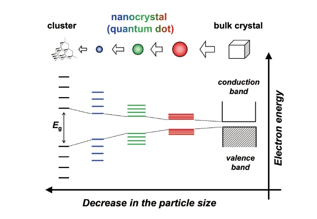
Fig. 1 Conceptual diagram illustrating how the quantum size effect influences the electronic energy structure of semiconductor nanocrystals (quantum dots).
Precise control over the optical properties of quantum dots requires accurate tuning of their shape and size. At present, quantum dots made of binary semiconductors such as CdS, CdSe, CdTe, and PbS are the focus of particularly active research efforts; this is due in large part to the relative ease with which high-quality quantum dots can be fabricated via the colloidal-synthesis method reported by Bawendi et al. in 1993, which used non-aqueous solvents and was one of the accomplishments honored by the 2023 Nobel Prize in Chemistry.4) Prior to this breakthrough, quantum dots had been synthesized by relatively simple methods—for example, by adding chalcogenide precursors at room temperature to dilute aqueous solutions containing metal salts, in the presence of stabilizers to prevent agglomeration of nanoparticles—that did not allow precise control over particle growth; most quantum dots produced by these methods were polydisperse. In contrast, the method developed by Bawendi's group was based on pyrolysis of precursors in hot organic solvents with high boiling points. In the first stage of this method, trioctylphosphine (TOP) containing precursors (dimethylcadmium and selenium) was rapidly injected via a syringe into trioctylphosphine oxide (TOPO) at 300°C, to synthesize CdSe crystal cores. Since the solution temperature suddenly decreased, the solution was then heated again to 230-260°C to continue crystal growth, yielding quantum dots whose sizes could be controlled by varying the heating time.4) This technique elegantly separated the processes of crystal nucleation and crystal growth, allowing highly precise control over the size of quantum dots while preserving their monodispersivity; for this reason it was widely adopted, and later became known as the hot-injection method. CdSe quantum dots produced by hot injection were high in quality and had only a small number of defect levels, ensuring band-edge photoluminescence with extremely narrow spectral linewidths. This finding opened the floodgates to a wealth of applications for quantum dots as highly monochromatic light-emitting components.
As noted above, the quantum size effect ensures that the electronic energy structure of quantum dots varies dramatically as the particle size is reduced, and achieving precise control over optical properties thus requires fabricating quantum dots with monodisperse particles. This has spurred the development of post-processing techniques for narrowing the particle-size distribution, allowing monodisperse particles to be obtained even from synthesis methods producing polydisperse distributions. This may be done using various analytical methods; examples include size-exclusion chromatography, which separates particles by size, and electrophoresis, which exploits the fact that the electric charge carried by a particle varies with particle size.3) An alternative technique, available only for nanoparticles, is size-selective precipitation, which exploits the highly sensitive size dependence of the solubility of quantum dots in solutions.4) In this method, small quantities of non-solvents are added to a solution in which quantum dots have been uniformly dissolved, inducing particles of larger sizes—and correspondingly lower solubilities—to aggregate and precipitate out of the solution. Chemical methods such as these are used to separate quantum dots purely by size, with no dependence on chemical composition or optical properties.
An alternative technique, which does use photochemical reactions to produce monodisperse quantum dots, is the method of size-selective photoetching developed by the author and collaborators.5) This approach is based on two phenomena: oxidative decomposition via light irradiation (photoetching) of metal chalcogenide semiconductors such as CdS or CdSe, and the increase in bandgap energy Eg with decreasing particle size due to the quantum size effect. When CdSe is irradiated by light, it undergoes photooxidative decomposition via the reaction

When chemically synthesized CdSe quantum dots are irradiated by monochromatic light at a wavelength just below the absorption edge, quantum dots of relatively larger sizes are selectively photoexcited and photoetched, causing the particle-size distribution to become concentrated at smaller sizes. As each particle decreases in size, its bandgap energy Eg increases due to the quantum size effect; eventually, the particle shrinks to a size at which it can no longer absorb the monochromatic irradiation light, at which point reaction (1) cannot proceed and the photoetching process terminates.
Figure 2a shows diffuse reflectance spectra of CdSe quantum dots synthesized by size-selective photoetching.5) After light irradiation, the spectra shift toward shorter wavelength; in each case, photoetching of CdSe quantum dots continues until their absorption onset matches the wavelength of the monochromatic irradiation. As the irradiation wavelength decreases from 630 nm to 460 nm, the synthesized CdSe quantum dots shrink in size from 4.3 nm to 1.7 nm. The photoetched CdSe quantum dots exhibit strong band-edge photoluminescence, with the emission peak wavelength shifting toward shorter wavelengths as the irradiation wavelength is decreased. This is illustrated by the photographs of Figure 2b, in which aqueous solutions containing photoetched CdSe quantum dots show bright photoluminescence under irradiation by ultraviolet light.
One advantage of size-selective photoetching is its ability to control the sizes of quantum dots in site-selective ways. When CdSe quantum dots are fixed in position on a glass substrate and selectively irradiated by monochromatic light through a photomask, quantum dots in irradiated regions undergo size-selective photoetching and shrink in size; these dots then exhibit more intense photoluminescence than dots in regions where photoetching is blocked by the mask, yielding clear contrast features in photoluminescence images (Figure 2c).
In summary, size-selective photoetching produces quantum dots with sizes determined by the irradiation wavelength, allowing dot sizes to be chosen and controlled with high precision. In principle, the method is applicable to any semiconductor exhibiting quantum size effects and susceptible to photoetching; in addition to CdSe, it has been used successfully to control the sizes of quantum dots made not only from other binary semiconductors, such as CdS6) and CdTe,7) but also from the ternary semiconductor AgInS2,8) one of the multinary semiconductors discussed in the following section.
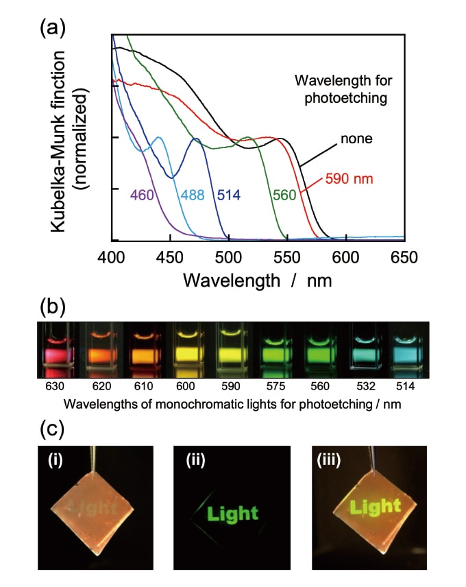
Fig. 2 (a) Diffuse reflectance spectra of CdSe quantum-dot films prepared by photoetching with monochromatic light of various wavelengths.
(b) Photoluminescence (under ultraviolet irradiation) from aqueous solutions containing CdSe quantum dots prepared by size-selective photoetching.
(c) Photographs of a CdSe quantum-dot film partially photoetched through a photomask via monochromatic irradiation at wavelength of 560 nm. (i) Under ambient indoor light. (ii) Under ultraviolet radiation. (iii) Under ambient indoor light with ultraviolet radiation.
Figure reproduced with permission from Ref. 5. ©2006 American Chemical Society
The quantum dots studied by researchers today are made primarily of binary semiconductors such as CdS, CdSe, or PbS. An advantage of these materials is that there exist well-established liquid-phase methods for synthesizing high quality quantum dots from them; however, because these materials contain highly toxic heavy metals such as Cd and Pb, their use is heavily restricted, complicating the development of practical devices based on these binary quantum dots. To address this problem, our research group is developing novel quantum dots based on multinary semiconductors composed of low-toxicity elements; in particular, we have successfully fabricated high-quality quantum dots from I–III–VI ternary semiconductors combining group-11, group-13, and group-16 elements. These compounds, which contain no highly toxic elements, have also been extensively studied as light-absorbing materials for thin-film solar cells.
We fabricated quantum dots composed of the solid-solution semiconductor (AgIn)xZn2(1- x)S2, a quaternary compound containing the elements Zn, Ag, In, and S, by alloying two semiconductor materials with similar crystal structures, that is, AgInS2 (bulk Eg: 1.8 eV) and ZnS (bulk Eg: 3.5 eV).9) We added silver acetate, indium acetate, and zinc acetate as metal precursors and thiourea as a sulfur precursor to oleylamine (OLA)—containing dodecanethiol (DDT) as a stabilizing agent (particle surface ligand) to prevent particle agglomeration—and stirred vigorously at 250°C to produce Zn–Ag–In–S quantum dots via thermal decomposition of the precursors. (We refer to this synthesis technique as a heating-up method.) We controlled the particle composition by varying the constituent fractions of the various metal ions in the ratio Ag:In:Zn=x:x:2(1–x). In contrast to the synthesis of binary-semiconductor quantum dots, the synthesis of quantum dots composed of multinary metal chalcogenides requires the use of multiple metal precursors, whose reactivity must be individually controlled to achieve precise control over the chemical composition of the resulting quantum dots. Indeed, the size, shape, and composition of multinary quantum dots are significantly influenced by synthesis conditions such as reaction temperature, reaction medium, type of ligands used, and choice of precursors, all of which must be carefully tuned to yield high-quality dots. Figures 3a,b show absorption and photoluminescence spectra of Zn–Ag–In–S quantum dots of various compositions, with an average particle size of about 5.5 nm. As the composition ratio x is varied from 1.0 to 0.1—thus increasing the Zn content—the bandgap energy Eg of the Zn–Ag–In–S quantum dots increases and the absorption onset wavelength shifts from 680 nm to 450 nm. These quantum dots exhibit broad photoluminescence peaks (with full width at half maximum (FWHM) of >100 nm) due to the presence of intragap defect levels. As Eg increases, the emission peak wavelength shifts from around 800 nm to 530 nm. DDT molecules are strongly adsorbed on quantum-dot surfaces through thiol groups, significantly affecting nanocrystal growth; increasing the DDT concentration in the reaction medium thus yields dots of smaller sizes, and this allows the average particle size to be controlled over the range 4–8.5 nm. Figure 3c shows photoluminescence of Zn–Ag–In–S quantum dots dissolved in chloroform under ultraviolet irradiation. The particle size and particle composition provide two distinct variables that can be tuned to adjust the photoluminescence wavelength, allowing the color of light emission to be controlled over a wide range of the visible spectrum from green to red. This tunability is not offered by conventional binary quantum dots.
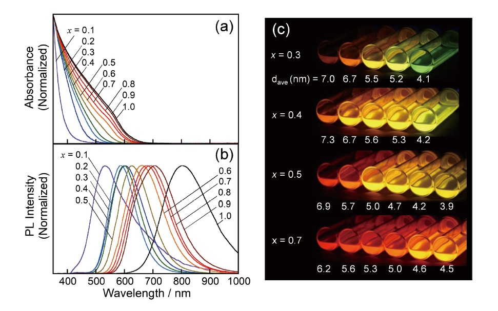
Fig. 3 Optical properties of Zn–Ag–In–S quantum dots synthesized with various chemical compositions x . (a) Absorption spectra. (b) Photoluminescence spectra. (c) Photographs of photoluminescence from quantum dots dissolved in chloroform under ultraviolet irradiation, with average particle size dave indicated in units of nanometers.
Figure reproduced with permission from Ref. 9. ©2015 American Chemical Society
As we observed for the example of Zn–Ag–In–S quantum dots, the photoluminescence peaks for I–III–VIbased quantum dots tend to exhibit broadening due to defect sites in the nanocrystals. When our group first began research on the development of multinary quantum dots, we supposed that the prevalence of defect levels would pose insurmountable hurdles to the goal of narrowing these luminescence peaks. However, we have since learned that precise control of the reaction conditions during liquid-phase chemical synthesis does in fact allow fabrication of high-quality I–III–VI quantum dots exhibiting only sharp band-edge luminescence peaks.10,11)
With careful control over the particle composition, AgInS2 quantum dots are observed to emit a narrow band-edge photoluminescence peak.11) We fabricated AgInS2 dots by reacting sulfur compounds with corresponding metal salts at 250°C in an OLA/DDT mixed solvent. The photoluminescence properties of the quantum dots produced in this way vary significantly depending on the metal ratio (Ag/In) of the precursors used; for Ag–In–S dots with a lower Ag fraction compared to the stoichiometric composition (Ag/In=1), we observe both a broad defect-site emission peak and a sharp band-edge emission peak at a shorter wavelength.11) The defect-site emission is due to intragap defect levels at the particle surface; to eliminate it, we covered the particle surface with gallium sulfide (GaSx) to yield Ag–In–S@GaSx quantum dots with core-shell structures. This almost entirely removed the broad emission peak, leaving only the narrow band-edge emission peak. We interpret this result as follows: covering the surface of an Ag–In–S core particle by a shell of GaSx—which has a higher bandgap energy Eg—results in the formation of a type-I heterojunction, eliminating defect levels at the core surface and ensuring that photogenerated electron-hole pairs remain effectively confined to the interior of the core particle.
I–III–VI semiconductors have the advantage of allowing easy formation of solid solutions by embedding same group elements in the interior of crystals, and this feature has been studied for use in fabricating semiconductor thin films with varying absorption properties. This strategy for tuning optical properties is applicable to multinary quantum dots as well, including quantum dots of I–III–VI semiconductors. When quantum dots are made of a solid solution of two semiconductors with different bandgap energies Eg, the Eg values of the dots lie between those of the two pure semiconductors and may be continuously varied by controlling the composition of the solid solution. We prepared quantum dots by alloying AgGaS2 (bulk Eg: 2.7 eV) with AgInS2 (bulk Eg: 1.8 eV) and demonstrated the ability to control the optical properties over a wide wavelength range of visible light.11) We fabricated Ag–In–Ga–S solid-solution quantum dots by adding gallium salts during synthesis; as the In/Ga ratio in the obtained dots decreases, the bandgap energy increases continuously from Eg=2.07 eV to 2.54 eV. Covering the particle surface with a GaSx shell yields Ag–In–Ga–S@GaSx core-shell quantum dots exhibiting sharp band-edge photoluminescence regardless of the In/Ga ratio, with the emission peak wavelength shifting toward shorter wavelengths as Eg increases (Figure 4). The photoluminescence quantum yield (PLQY) attained a maximum value of 28% for dots showing a band-edge photoluminescence peak at 530 nm (FWHM: 41 nm). Further improvements in synthesis techniques for multinary quantum dots enabled further increases in PLQY; to date the highest value yet achieved is 75% for quantum dots emitting sharp green band-edge photoluminescence with a peak wavelength of 543 nm and a FWHM of 37 nm.12)
For Ag–In–S-based solid-solution quantum dots, several strategies exist for shifting the optical response toward longer wavelengths; this may be done, for example, by replacing S with Se, or replacing Ag with Cu, to decrease Eg. As a first step, we replaced group-16 elements with Se to fabricate Ag–In–Ga–Se solid-solution quantum dots exhibiting band-edge photoluminescence in the near-infrared wavelength region. We used selenourea as a chalcogen compound together with corresponding metal salts and synthesized Ag–In–Ga–Se quantum dots via pyrolysis at 300°C in an OLA/DDT mixed solvent.13) The surfaces of these dots were further coated with GaSx shells to yield core shell particles as described above. The Ag–In–Ga–Se@GaSx core-shell dots obtained in this way exhibited intense band-edge photoluminescence, with the peak emission wavelength blue-shifting from 890 nm to 630 nm as the In/Ga ratio was reduced to increase Eg. The maximal PLQY was 14%, achieved for dots with a peak emission wavelength of 800 nm. Control over the photoluminescence wavelength can also be achieved by forming a solid solution between semiconductors containing different group-16 elements, that is, S and Se: we fabricated Ag–In–Ga–S–Se quantum dots and observed the emission peak wavelength shifting toward a longer wavelength—from 580 nm to 790 nm—as the Se/S ratio in the dots was increased.14) These results demonstrate the extensive tunability of Ag-based I–III–VI quantum dots: by varying the choice and relative abundance of group-13 and group-16 elements, the emission peak wavelength can be adjusted over a broad range—extending from the visible to the infrared—while preserving a narrow band-edge emission peak.
One application of photoluminescent quantum dots is as light-emitting probes for bioimaging. The near-infrared wavelength band 700-1870 nm has been termed the “biological window” due to the high optical transparency of biological tissue in this range, and the ability to fabricate highly photoluminescent quantum dots with low-toxicity materials allows the realization of powerful new fluorescent probes for biological tissue imaging. We have demonstrated this new approach to photoluminescent bioimaging by embedding Ag–In–Ga–Se@GaSx core-shell quantum dots—prepared as described above (peak luminescence wavelength: 821 nm)—in liposomes, then dissolving in aqueous solution and injecting subcutaneously into mouse specimens.13) Figure 5 shows near-infrared photoluminescence images superposed with X-ray CT images for such a specimen. The quantum dots emit intense near-infrared photoluminescence from the interior of the organism, with the emission intensity increasing as the quantum-dot concentration increases; the images indicate that the injected quantum dots are dispersed over a region extending to a depth of roughly 5 mm beneath the skin of the specimen.
Replacing Ag with Cu yields Cu–In–Ga–S quantum dots with lower Eg values than Ag–In–Ga–S dots. We used copper acetate (II) as a group-11 precursor and obtained Cu–In–Ga–S quantum dots via thermal decomposition at 300°C in an OLA/DDT mixed solvent.15) Increasing the In fraction in these dots decreases Eg from 2.77 eV to 1.74 eV, shifting the photoluminescence peak wavelength from 625 nm to 740 nm. The FWHM of the emission peak is 0.23 eV, significantly narrower than those (>0.40 eV) reported previously for Cu–In–Ga–S quantum dots; however, the emission lifetime is relatively long—in the range 200-400 ns—due most likely to photoluminescence from defect levels. The maximum PLQY is 8.3%, observed for Cu–In–Ga–S quantum dots showing an emission peak near 600 nm; covering the surfaces of Cu–In–Ga–S dots with GaSx, or with Ga–Zn–S, increased the PLQY to 27% or 46%, respectively, without significantly affecting the peak wavelength or the peak width.
Light-emitting diodes (LEDs) fabricated with quantum dots with controllable emission wavelengths have been widely studied for applications including lighting and display devices. These devices, which consist of thin layers of highly luminescent quantum dots sandwiched between electron-transport layers and hole-transport layers, are induced to emit light electrically by applying an external voltage; this process is called electroluminescence. Figure 6 shows an electronic energy diagram, photographs of operating devices, and measured electroluminescence spectra for red LEDs fabricated with Cu–In–Ga–S quantum dots.15) For comparison, electroluminescence spectra are plotted together with photoluminescence spectra of Cu–In–Ga–S quantum-dot thin films; the electroluminescence spectra exhibit peaks at the same emission peak wavelengths as the PL spectra, but additional emissions are also present at the longer wavelength side of the main peak due to defect levels with lower energy. These defect emissions are produced by externally-injected charge carriers captured by defect states in quantum dots. Our research group has used similar methods to fabricate LEDs emitting light at various colors, including yellow-emitting devices fabricated with Ag–In–S quantum dots16) and green-emitting devices prepared with Ag–In–Ga–S quantum dots.17,18) These findings demonstrate that multinary quantum dots with narrow photoluminescence peaks can be used to achieve vivid electroluminescence. Furthermore, the ability to tune the emission wavelength over a broad range makes multinary quantum dots promising candidate materials for full-color devices, exploiting their unique properties.
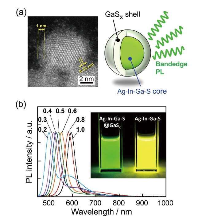
Fig. 4 (a) HAADF-STEM image (left) and schematic illustration (right) of an Ag–In–Ga–S@GaSx quantum dot with core-shell structure.
(b) Photoluminescence spectra of Ag–In–Ga–S@GaSx quantum dots with various core compositions. Curves are labeled by the In/(In+Ga) ratio used in synthesizing the core
particles.
Figure reproduced with permission from Ref. 11. ©2018 American Chemical Society
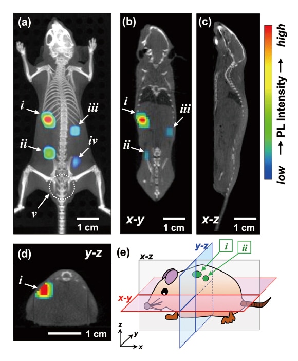
Fig. 5 (a-d): 3D near-infrared photoluminescence images of a mouse specimen following subcutaneous injection of Ag–In–Ga–Se quantum dots. Images are superpositions of X-ray CT scans and PL images.
(e) Schematic illustration indicating configuration of the mouse specimen for imaging.
Figure reproduced with permission from Ref. 13. ©2020 American Chemical Society
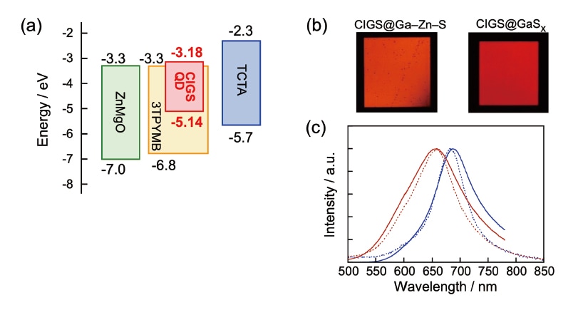
Fig. 6 LEDs fabricated with Cu–In–Ga–S (CIGS) quantum dots as a light-emitting layer. (a) Electronic energy diagram. (b) Photographs of operating LED devices. (c) Electroluminescence (solid curves) and photoluminescence(dashed curves) spectra for the devices prepared with CIGS@Ga–Zn–S (red curves) and CIGS@GaSx (blue curves).
Figure reproduced with permission from Ref. 15. ©2023 AIP Publishing
The ability to tune the optoelectronic properties by controlling the particle size has made quantum dots a focus of intense current research targeting applications to photo-functional devices. However, to date most studies have used quantum dots composed of binary semiconductors containing highly toxic heavy metals, making them difficult to develop for practical applications. This has created a need for new types of quantum dots composed of low-toxicity materials, with one promising candidate being multinary semiconductor quantum dots containing three or more elements. The optical properties of such multinary dots depend both on the particle size and particle composition; this dual-parameter control is a key feature of multinary quantum dots not offered by conventional quantum dots made of a binary material such as CdSe. Thanks to rapid recent advances in liquid-phase synthesis methods, it is now increasingly possible to fabricate high-quality multinary quantum dots composed of low-toxicity elements; as the breadth of applications for such quantum dots continues to expand, we are confident that, in the near future, these materials will not only find uses in a growing range of practical devices, but will also play key roles in the exploration of novel photofunctional materials.
References
See more
