Future technologies and that possibilities, as envisioned by the young researchers of today
Prof. Makoto Kuwahara is working on developing spin-polarized pulse-transmission electron microscopy at Nagoya University. Dr. Tadahiro Kawasaki is developing aberration correctors at Japan Fine Ceramics Center (JFCC). Dr. Kazuo Yamamoto is engaged in research on electron holography, also at JFCC.
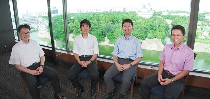
We invited several young researchers in their 30's and 40's, all working on researching and developing next-generation technologies for electron microscopy, to discuss their opinions on how electron microscopy will evolve and how their works and visions will help drive that progress.
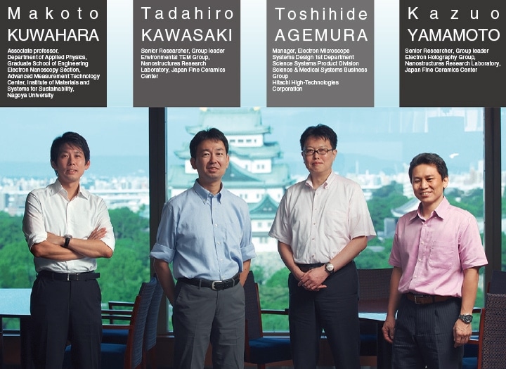

Associate professor, Department of Applied Physics, Graduate School of Engineering Electron Nanoscopy Section, Advanced Measurement Technology Center, Institute of Materials and Systems for Sustainability, Nagoya University
I am working on developing a new type of electron microscope that uses a photocathode as the electron source which generates novel electron beam. Using this technique, we are challenging to observe fine-structures that were previously invisible via spin-resolved and time-resolved measurements. Spin is a degree of freedom for an electron. One way to think about spin is to picture the rotational motion of a spinning top that can only be in two states, which are called up and down. By illuminating spin-polarized pulse-beam to a specimen, we obtain not only three-dimensional spatial information but also the temporal and spin information, which can add new functions and enhance the capabilities of electron microscopy.
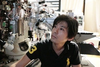
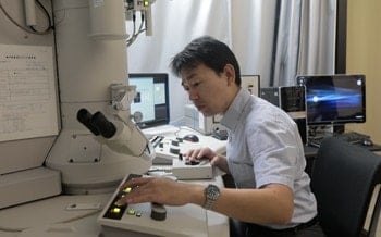
Senior Researcher, Group leader Environmental TEM Group, Nanostructures Research Laboratory, Japan Fine Ceramics Center
My research can be broadly divided into two areas. One is for improving the resolution of scanning electron microscope (SEM) images by developing technologies for correcting aberrations, which causes blurring in images. The goal is to develop a simpler, more compact, and more affordable product than the ones available today and installed in general-purpose SEMs. Currently, we're collaborating with Hitachi High-Tech on a project for the Japanese government*1. The second area of my research is In-situ observation using environment electron microscopy. We have been developing technology to allow real-time observation of samples immersed in gases or liquids, which enables direct observation of phenomena, such as catalytic reactions in gases or electrochemical reactions inside batteries.
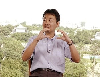
Senior Researcher, Group leader Electron Holography Group, Nanostructures Research Laboratory, Japan Fine Ceramics Center
I've been studying electron holography since I was a doctoral student. Electron holography is a type of transmission electron microscopy that exploits the wave nature of the electron and the corresponding interference phenomena to make direct observations of the electric and magnetic potential inside materials. I have worked on technical research to yield simultaneous improvements in the sensitivity and spatial resolution of electron holography, as well as relevant applications such as the observation of magnetic nanoparticles. It has been 20 years since I began this research, and I still find that the measurements using electron holography are extremely interesting—I'm a long way from getting bored! For the past 10 years or so, I've been working to observe lithium-ion batteries, focusing on solid-state lithium-ion batteries, which are a promising next-generation battery due to their high energy density and safety performance. Lithium is a light element—its atomic number is just 3—so it scatters electrons only weakly, and in the past, it was not easy to observe distributions of lithium, or how they varied. But then I wondered what If we focus on the changes in electric potential that arise when lithium ions enter and exit the electrodes? That was the beginning of In-situ observations of lithium-ion batteries using electron holography.
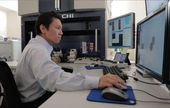
Manager, Electron Microscope Systems Design 1st Department Science Systems Product Division Science & Medical Systems Business Group
Hitachi High-Tech Corporation
Interviewer
I've been involved with R&D in scanning electron microscopy (SEM) for a long time, starting with field-emission SEM (FE-SEM). Presently, I'm part of the Electron Microscope Systems Design 2nd Department and am working on the development of 120 kV transmission electron microscopes (TEMs). Today I'm interested in some possible directions for next-generation electron microscopes. As an engineer, I am hoping that we get to delve deep into the subject.
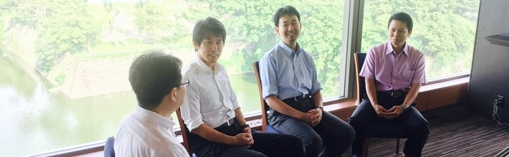
Agemura: Today we've invited several young researchers working on developing the next generation of electron microscopes. They shall be asked to explain how electron microscopy will evolve going forward and to share with us their visions for what possibilities lay ahead. In fact, I graduated from Nagoya University myself and I am in the same generation as the guests, so I hope to hear your honest opinions.
So, each of you has participated in collaborative R&D projects with us at Hitachi in the past. I'd like to hear about those projects and how you got started. Let's start with Dr. Kawasaki, who will tell us about techniques for correcting aberration.
Kawasaki: Well, the technology itself goes back to the ideas of Professor Takashi Ikuta from Osaka Electro-Communication University, and in fact it's something I've been working on ever since my days as a student. The idea is to correct spherical aberration using just two electrodes—one is an annular electrode and another is a circular electrode. We have been developing a way to apply this idea to electron microscopes.
Agemura: I attended a conference and saw the presentation you gave on this technology. At the time, I was working on the development of FE-SEM and I thought that it could probably be applied to SEM as well. I asked you what you thought after your talk, and I was struck by how simple the method was compared to conventional techniques for aberration correction, and also by how small the corrector was. Now, the results have been coming little by little.
Kawasaki: Using this method, you may not be able to achieve the absolute highest resolution, but I think that the device is very easy to use and a simple way to increase resolution. At the moment, we are only using it for SEM, but eventually I expect to apply it more widely, such as to TEM and lithography.
We're at a point where we are just a step or two steps away from the result. The only remaining challenge is how to align the aberration corrector to the SEM optical axis. We've been conducting many experiments on this technology for obtaining some good results at least sometime in this fiscal year.
Agemura: Professor Kuwahara, when did you first become involved with Hitachi?
Kuwahara: When I studied on development of accelerators for experiments in elementary particle physics as a Ph.D. student, I worked together with Hitachi on research investigating methods for generation of spin-polarized electron beam. Because, my advisor, Professor Tsutomu Nakanishi, was using Hitachi's optical system for electron microscope and spin manipulators. Since then, we have had many useful conversations regarding research on electron sources, and we have pursued research collaborations in that direction as well. I started doing research in the field of electron microscopy about seven years ago.
Yamamoto: I also have been working with Hitachi since I was a student in Professor Takayoshi Tanji's laboratory at Nagoya University. Professor Tanji had been involved in a Japan Science and Technology Agency ERATO project called the "Tonomura Electron Wavefront Project" (1989-1994), and he had a major impact on the results of that research project. I have read some books written by Dr. Akira Tonomura, who was a Director of Research at Hitachi at the time, and saw the results of Dr. Tsukasa Hirayama (now at JFCC) on the observation of magnetic fields in barium ferrite particles. This idea that electron holography was used for visualizing electric and magnetic potential in microscopic regions had a huge impact on me. After I joined JFCC, I was fortunate to receive invaluable assistance from Dr. Yoshifumi Taniguchi in Hitachi for developing our new electron holography microscope. I am grateful to him for helping us perfect this outstanding and unique instrument.

Agemura: Professor Kuwahara, when I first saw your spin-polarized pulse setup, I remember thinking it had great potential as an electron source. Indeed, it was the world's first trial of the idea itself—irradiating a sample with spin-polarized electrons and observing the spin-polarized electrons thus produced. Moreover, the energy bandwidth (the range of fluctuation in the energies of electrons) was low, at just 0.24 eV, and the brightness was high—and I thought it was an amazing technology. Theoretically, is it possible to reduce the energy bandwidth even further?
Kuwahara: I think it's possible. If we can find better operating conditions, I think we can achieve energy bandwidths below 0.1 eV. Moreover, there is the additional advantage that we accelerate the fi nal voltage in a single step, without using an extractor electrode. This means we can increase the number of electrons squeezed into a single pulse.
Agemura: As you know, the extractor electrode in a field-emission electron gun creates the voltage at the emitter surface (a thin single-crystal tungsten anode) for emitting electrons; typically, voltages of 3.5-5 kV are required. However, a pulsed electron source does not require an extractor electrode, so there is no need to move the position of the light source, making it extremely stable. Dr. Yamamoto, we're looking forward to further reductions in the energy bandwidth.
Yamamoto: Is there any research related to spin-polarized TEM and/or SEM?
Kuwahara: There is research on spin SEM. However, the incident beam consists of ordinary unpolarized electrons, and the magnetic structure is observed by measuring and mapping the spin-polarization of the secondary electrons. I haven't seen any attempts to use spin-polarized electrons for the incident beam.
Agemura: It is diffi cult to achieve spin polarization because we need to circularly polarize and control the laser. Thus, it can help differentiate products. Some Hitachi researchers are studying spin, so I expect the fi eld of applications to expand further.
Kuwahara: One more thing is that our advantage in the time-resolved measurement comes from the ability to produce coherent pulsed electron. I expect that it should be possible to observe the dynamics of phase information as well.
Agemura: The mention of phase information leads us into a discussion of holography, and I'd like to ask Dr. Yamamoto to speak on this. I am not very familiar with electron holography, but I understand there have been attempts to observe phase information or electric field information in areas such as ptychography or 4D scanning transmission electron microscopy (4D-STEM), which achieves high-resolution imaging using effectively 4-dimensional information captured by a pixel detector. How does this differ from electron holography?

Yamamoto: Recently, we have been observing electric fields in the same semiconductor sample using the electron holography and STEM-based differential phase-contrast (DPC) method by using the same sample. An advantage is that the electron holography is excellent for quantitative purposes. For example, measurements of the potential distribution in the semiconductor device require quantitative characterization and feedback to the device processing. As for drawbacks, I guess you could cite the inconvenience. From the perspective of making simple measurements, it's probably better to use STEM, which everybody is already comfortable using. Electron holography also has limitations due to electron interference, and one is restricted to observing only the edges of samples.
The STEM-based observation techniques such as ptychography, 4D-STEM or DPC are cur rently in a transitional R&D phase, but in the future, I expect that they will be widely used for compensating the theory and electron holography measurements.
Agemura: Like electron holography, In-situ observation is expected to become an important visualization technique. Dr. Kawasaki, how did you involved in making In-situ observations?
Kawasaki: The topic of my research when I was a student was the development of aberration correction technology for TEM, and the samples we were observing at that time were catalytic nanoparticles. We were trying to analyze the atomic structures of these samples using aberration-free phase imaging.
However, at the time, we could only observe catalysts in vacuum. I thought it would be nice to observe catalysts in the process of reacting, and I started to do research on this topic when I moved to Nagoya University. For the purpose of this research, I had modifi ed a Hitachi H-8000 transmission electron microscope by hand to allow the injection of gas.
Kuwahara: Regarding In-situ observations, I think the spin-polarized pulses we were just talking about could be useful. With other methods, reducing the measurement time means reducing the number of electrons (the dose) used for the measurement, and that makes observations difficult. However, with our method, it is possible to increase the number of electrons in each pulse, thus increasing the time resolution. We're hopeful that this will allow us to observe the dynamics of phenomena that we still haven't been able to observe.
Agemura: It seems the various topics we're discussing today are interrelated in a variety of ways. At the moment, we at Hitachi are pursuing separate collaborations with each of you individually, but in the future, it would be great if we could combine these projects. We're looking forward to making that happen.
Agemura: All of you have been kind enough to use Hitachi's electron microscopes in your research thus far. Please let me use this opportunity to hear your thoughts.
Kawasaki: I would like to develop unique instruments that do not exist anywhere else and are customized for my experiments. It would be great if there could be a framework in which Hitachi could help us to realize our ideas.
In particular, one problem we're facing with In-situ observations right now is that electron-beam irradiation tends to transform the sample in various ways. Ideally, we would like to observe the sample as is, without applying an electron beam. Of course, that's impossible, but we're wondering if it might be possible to use pulses to achieve some sort of strobe observation utilizing the contrast between the conditions when the electron beam is on and off. This may realize a new type of In-situ observation that minimizes the effect of the electron beam.
Yamamoto: In my opinion, Hitachi's electron microscopes are incredibly easy to use—the fact that pretty much anybody can use them is a major advantage. In the future, it would be necessary to add interfaces that can be operated naturally by people who grew up in the smartphone era.
For an example, you could offer a smartphone-like interface in which the operator uses a touchscreen to select regions of images to enlarge or enter data. That would be really revolutionary. By making everything digital, the instrument should become easier to use. I've been sharing this idea with all sorts of different people for the last four years, and I'm looking forward to finding out which instrument manufacturer will be the fi rst to incorporate my proposals.
Agemura: That's fascinating. The American TV drama Star Trek: The Next Generation (1987) adopted a touchscreen panel as the control interface for its spaceship back in the 1980s. I think that sort of imagination—to be able to anticipate the technologies of the future—is incredibly important. We will defi nitely look into your ideas.
Kuwahara: For my personal case, before I took apart and reassembled that Hitachi instrument, I had barely touched a TEM, but now techniques for correcting aberration—which has been an issue thus far—are advancing, and I think the next big areas for improvement will be electron sources and detectors. Hitachi is a technological leader and I'm hoping Hitachi will develop a new, revolutionary electron microscope that will take the world's breath away.
Yamamoto: For the electron source in particular, we've been using old technologies for a really long time, and surely the time has come to modernize. For example, magnetic-field superposed fi eld-emission electron guns, in which a magnetic field is superposed to focus the beam, was developed by Hitachi when I was a student, but I don't think it has been designed into any general-purpose instrument yet. I think you could make higher performance products by incorporating features like this.
Agemura: As far as electron sources are concerned, we know Professor Kuwahara's electron beam has high interference, and we are very excited to use it.
Kuwahara: The relevant question is how can compact and easy-to-use instruments be made? As a pre-processing step, it's necessary to deposit an alkali-metal to semiconductor surfaces. This requires an additional vacuum chamber, creating new projected devices, which are not present in a standard TEM. The challenge is downsizing the devices and creating a compact form. Also, the optical source system focuses a laser to be about 1 µm diameter. This part defi nitely needs to be made smaller as well.
Yamamoto: If we could collaborate to improve the format of devices like this and achieve signifi cant improvements in brightness, we would change the world in major ways.
Kawasaki: Of course, this will require some time—after all, even Professor Tonomura spent 10 years developing field-emission electron microscopy.
Agemura: Regarding the electron source, this will require material design, so the development process will take some time. Still, we should attempt to accelerate the pace of research. I hope we can continue to work together in the future to advance the state of research in pursuit of increasingly better electron microscopes.
Agemura: Next, I'd like to get your views on how electron microscopes should evolve going forward. I'll ask each of you to describe the sort of electron microscope you're seeking.
Kuwahara: If we compare optical microscopes to electron microscopes, the optical case has the upper hand when it comes to squeezing more particles into the beam, but with electrons we can take advantage of interactions between charged particles, which allows us to observe fi ner features. I think it's important to explore this point further.
I remember the first time I felt truly excited to be doing electron microscope research was when I saw that electron beam waves were aligning with each other and that the electrons they controlled were producing images. Until that point I had been doing elementary particle research, and I hadn't thought much about the wave aspects of what happens when you pack electrons into a beam and hit a sample with them. I think it's incredibly fascinating that we can actually see the effects of wave interference before our very eyes, for example in holography.
Of course, if you want to use light to look at things in fine-grained detail, you could always use an X-ray microscope, but these are huge instruments, whereas electron microscopes can be made small enough to fit in a laboratory. For the purpose of accelerating the pace of research, I think it's crucial to have instruments available to use every day in each and every institution. In this sense, I think I need to achieve a more compact footprint for my own instrument.
Kawasaki: From the perspective of my work on In-situ observations, it would be great if it were possible to open up the space around the sample, like in optical microscopes. I think this would allow us to do more complicated experiments. For high-resolution TEM and STEM, the sample has to be located in a vacuum chamber just a few millimeters in size. This makes it difficult to do things like inserting probes, heating or cooling, or otherwise manipulating the sample in conjunction with observing them. Of course, expanding the space around the sample has the drawback that the resolution would decrease. In the future, I hope it will be possible to build an electron microscope in which the sample space is enlarged but high resolution is retained by improving aberration correctors. That would enable us to do many more interesting experiments.
Yamamoto: Looking back at the history of microscopy, optical microscopes have been around for much longer than other types of microscopes. Many different ideas, and software, have accumulated in that field, and fields of research that use light or radiation beams are extremely advanced. My view is that we need to borrow ideas from these outside fi elds and bring them into the world of electron microscopy. I've actually done this myself, and I actively try to avoid getting trapped in the world of electrons by participating in research associations and conferences involving various different types of imaging technologies. In the fi eld of optical microscopy, I'm working on something called super-resolution, in which we try to go beyond the conventional limits of spatial resolution. It would be nice if something similar could be done for electron microscopes as well.
Agemura: As you say, I think it's important to learn techniques from other fields. For things like measuring radiation, the quantity to be measured is clear, and this has spurred advances in detectors. For example, in the past, people used silicon-lithium semiconductor detectors, but now silicon drift detectors (SDDs)—which can measure larger numbers of X-rays—have come to dominate the field. This is the sort of idea that could be found in books even 20 years ago. So, it's incredibly important to catch up with outstanding technologies of other fi elds and bring them into our own.
Agemura: To finish our discussion today, I'd like each of you to fantasize a bit: Suppose that, in the future, the ideal electron microscope becomes available. What would you use it to observe?
Kuwahara: Well, for me, one dream would be to make detailed observations of magnetic states inside samples and view them in the form of movies. If spins could be captured in three dimensions, that would be truly revolutionary. Another would be to bring quantum physics into an electron microscope for observation. If an entanglement state of the vacuum state and the one electron state is illuminated to a sample, it should be possible to detect information of the sample in the absence of the electron beam. By doing this, I think it would ultimately be possible to make measurements without damaging the sample.
Kawasaki: I'd like to observe chemical reactions directly. At present, we can use environmental microscopes to observe samples in gaseous environments, but we can't capture the motion of gas molecules. If it were possible to observe something like this directly, it should be possible to capture the moment at which a carbon monoxide molecule and an oxygen molecule react to form carbon dioxide. The ideal situation would be to observe details of the processes by which molecules react to transform into other molecules—that would really clarify everything.
In terms of technology, as I mentioned previously, I think an important question will be to how to minimize the interactions due to electron-beam irradiation. This will require improving every aspect of the instrument—the spatial resolution, time resolution, detector sensitivity, and performance of the electron source—but ultimately I hope to see the creation of such an electron microscope.
Yamamoto: I want to use electron holography to observe phenomena totally different from the magnets and semiconductors we can observe. One example would be biological organisms. In living creatures, muscle movements are controlled by electrical signals. In other words, electricity flows through nerve cells in the body, and this should give rise to variations in the electric potential. I want to observe these variations while, for example, focusing on a moving muscle.
Of course, this would require collaborating with biology researchers. Ultimately, I'd like to know why living organisms stop moving when they die. How does energy get converted into variations in electric current to move the body? My dream is to use electron holography to answer these fundamental questions about living organisms. If this were possible, then maybe in the future we could use a microchip or something to send electrical signals to specific portions of a patient's body, and thus—for example—restore sight to a blind person. The research in which I've been involved thus far has been focused on only industrial applications, but in the future, I'd like to work on things that are more useful to the general public, in fields such as health and medicine. After all, charting paths through new territory that nobody has yet explored—that's the best part of doing research.
Agemura: Observing the dynamics of living organisms sounds like a fascinating idea. Making it happen will probably require answering important questions about how to minimize damage to the sample, as Dr. Kawasaki said; maybe Professor Kuwahara's spin-polarized pulses will be useful here. Today we were treated to a fascinating discussion of the future of electron microscopy. Thank you all for giving us so much of your time, and I look forward to working with you again in the future.
(Layout and text: Madoka Tainaka)
Editor's note
Some of the analogies I've heard to describe the process of electron microscopy include the following. "The resolution is equivalent to seeing a silver coin on the earth—from the moon." "Looking for the region you want to observe is the equivalent of finding a single needle in a school playground." On top of this, there is no guarantee that the silver coin or needle is actually even there. And yet nonetheless you go about the business of aligning the focus, always believing beyond a shadow of a doubt that what you're seeking is there. This is what research is all about. The evolution of microscopes has directly accelerated research in medicine and many other fields, and it's thrilling to imagine what sorts of instruments will be invented next by these professors—who entertained us today with their discussion on the future of electron microscopy.
(Reporter: Tomoe Otsuka)
See more
