The discovery of superlattice structures in perovskite crystals
SI NEWS Vol. 62-1 included an article titled “Role of FIB and TEM in Organo-Halide Perovskite Solar Cell Observations,” in which author Satoshi Uchida, a professor at the University of Tokyo, described important discoveries resulting from observations of perovskite thin films.
To learn more about the development of these next-generation solar cells that have captured the world’s attention, we visited Professor Uchida’s laboratory at the University of Tokyo Research Center for Advanced Science and Technology in Komaba, Tokyo.
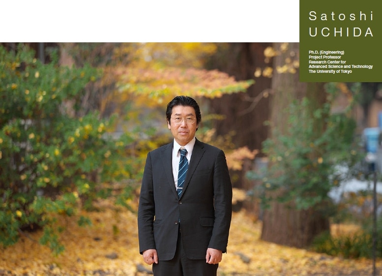
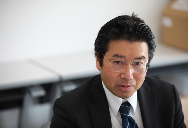
Satoshi Uchida, Ph.D. (Engineering) Project Professor Research Center for Advanced Science and Technology The University of Tokyo
Worldwide production of renewable energy is increasing yearly, and forecasts from the International Energy Agency (IEA) and research institutes in various countries predict that renewable-energy production in 2030 will be two to three times greater than 2016 levels (Energy Whitepaper 2018, Japanese Ministry of Economy, Trade, and Industry). With the problem of global warming being a subject of growing concern around the world, advances in renewable energy, and solar power in particular, are eagerly anticipated.
As a child, Satoshi Uchida idolized his father—a chemistry researcher—and dreamed of becoming a PhD scientist in pursuit of truth. Eventually, as Assistant Professor at Tohoku University, Uchida took the first steps on his journey as a researcher in the fields of metallic materials and photocatalysts; by the time he had fulfilled his dream, Uchida knew in his heart that his goal was for the scientific truths he pursued to prove useful for society at large. This gave Uchida an interest in energy-related research, and it was in this frame of mind that he came across a 1991 research paper on dye-sensitized solar cells—whereupon, with the unshakable researcher’s intuition that this was going to be big, Uchida began his own work on the topic. “To be honest, at the time there wasn’t a lot of evidence to support my certainty that this would be a worthwhile endeavor,” Uchida admits, “but in retrospect I was fortunate to get involved at that early stage.”
At first, Uchida wasn’t even sure how to characterize the solar cells he assembled himself. With no knowledge, no experience, and no research funding—with nothing, in fact, but pure motivation—Uchida knew he might be just spinning his wheels, but remained undaunted in his passion to work on dye sensitivity, and swore to make the field his own.
All of this was happening during the early days of the Internet, which had not yet come into widespread use, but which was available to university researchers. “That was what I used to start announcing results,” recalls Uchida.
From results of trial-and-error experiments in his own research to analyses of trends in articles by overseas researchers, Uchida continued posting information resources related to dye sensitivity until the number of accesses to his website exceeded 1,000 per day—an extraordinary number for a site devoted to a restricted range of research topics, no matter how closely followed. As there were not enough researchers in Japan to explain the site’s popularity, Uchida reasoned that much of the interest must be coming from overseas. And, as the site began to attract more and more interest, a variety of information sources naturally accumulated, and research proceeded apace. Still, the project remained a lonely labor of love, spearheaded by a single researcher at Tohoku University.

Dye-sensitized solar cells and
their ability to incorporate colorful designs
It was around this time that Uchida received an invitation from Professor Hiroshi Segawa (Department of General Systems Studies, Graduate School of Arts and Sciences, University of Tokyo), his current boss, to pursue his studies at the University of Tokyo. Segawa, like Uchida, had been studying dye sensitivity since the early days of the field, and was among the researchers seeking practical applications of the technology. This was right around the time that Japan’s national universities were incorporated, and Uchida moved to the University of Tokyo in 2006, where he has now been conducting research for more than 10 years.
At the time of Uchida’s move, renewable energy had begun to attract significant interest—and high expectations—from society at large, and research on dye-sensitized solar cells had developed considerably. After all, dye-sensitized solar cells not only had the advantage of being made from environmentally-friendly materials, but were also dazzling in appearance, with adjustable colors and the ability to incorporate arbitrary designs.
During the 2011 Tohoku earthquake and tsunami, Uchida’s organization provided disaster-stricken regions with rechargeable portable LED lights equipped with dye-sensitized solar cells, a contribution that was gratefully received. In the immediate aftermath of the calamity, Uchida discussed with Segawa’s laboratory what they could do to contribute; the discussion led to a design for portable LED lights and a rapid collaboration with a manufacturer to produce 100 units, which were distributed at two sites (the cities of Sendai and Ishinomaki) in affected regions of Japan’s Miyagi prefecture. It was Uchida himself—a native son of Tohoku—who observed the disaster sites and selected the evacuation sites at which to distribute the LED lights. The lights came in handy at evacuation sites struggling to provide nighttime illumination, and disaster victims were delighted to receive them.
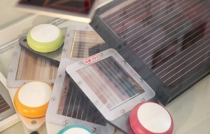
Portable rechargeable LED lights distributed in
disaster areas
Thus, dye-sensitized solar cells were a research project he was passionate about; one development that led to a particular breakthrough in the field was the 2009 proposal of perovskite solar cells. Although these devices boast the advantage of nearly twice the power-generation efficiency of dye-sensitized cells, Uchida was hesitant due to the use of lead as a material, which poses risks of harm to the human body. Eventually, however, Uchida joined the field of perovskite research, “a couple of rounds late,” as there was no sign that the direction of research that had suddenly changed would change again.
With large numbers of researchers pursuing enhanced power-generation efficiency through improved materials and structures, Uchida focused on a subject that had not previously been central to their research: the origins of, and conditions necessary for, high efficiency, and an exploration of the principles underlying power generation itself.
One example: methods for computing power-generation efficiency. Efficiency had conventionally been computed based on I-V curves, obtained by measuring current flows while adjusting voltages. However, in perovskites one obtains different, inequivalent curves depending on whether one is increasing or decreasing the voltage. This gives two distinct values for the power-generation efficiency, and one cannot be sure which is correct. This is a phenomenon unique to perovskites, not seen in silicon-based solar cells, and the question of why it occurred was not understood.
Whereas silicon-based cells comprise just two types of material—namely, P-type and N-type semiconductors—perovskite cells were constructed by stacking 5 layers of materials, one of which was the perovskite. Uchida focused on this point and discovered that the capacitance at the interfaces between layers was responsible for trapping large numbers of electrons—an order of magnitude more than in two-layer silicon cells. Thus, measured I-V curves could be separated depending on whether electron charging or discharging occurred during efficiency measurements.
At first, the research community favored an alternative explanation involving the motion of ions; however, with the announcement of Uchida’s paper in 2017, it became possible for the first time to demonstrate the reproducibility of separated I-V curves. Today, the question of how to reduce the electron-pooling (hysteresis) effect has emerged as a new research topic.
Starting around the year 2015, Uchida also began observing perovskite crystal structures. Before this, Uchida had paid several visits to Hitachi High-Tech’s Naka-Area Science Laboratory (in the city of Hitachinaka in Japan’s Ibaraki prefecture) for assistance from Hitachi engineers with focused-ion-beam (FIB) processing of specimens and observation and imaging via transmission electron microscopy (TEM).
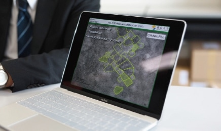
Image showing the coexistence of tetragonal and
cubic crystal structures
It was one day in November 2016 that the first sample was observed. Upon inspecting high-magnification TEM images of a perovskite sample, Uchida used the mouse to select certain subregions for scanning and electron-beam diffraction (EDS) imaging. The results were striking: in the region surrounding a hexagonal pattern of spots, miniature hexagons jumped out at him in satellite-like configurations. The larger hexagons fell within the range of expectations, but it was the smaller hexagons that gave Uchida goosebumps: “I just saw something amazing!”
“As soon as I saw those hexagons,” Uchida recalls, “I knew I something incredible was going on.” What he had seen that day in the perovskite layers of his sample was a structure in which multiple unit cells of an underlying crystal lattice repeat in a distinct pattern, with a spatial period several times longer than that of the unit cell—a structure known as a superlattice.
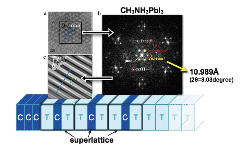
Figure 1: Observation of superlattice structure in a thin film of CH3NH3PbI3 perovskite.
(a) TEM image. (b) EDS image. (c) Fourier-transform image.
The significance of Uchida’s superlattice discovery was threefold. First, whereas perovskite crystals at room temperature had been thought to exist in a single, unique crystal structure—namely, the tetragonal structure—Uchida’s new result demonstrated that in fact this phase could coexist with the high-temperature cubic crystal structure, in which the spacings between atoms are slightly different. This much alone would have sufficed to overturn conventional wisdom, but Uchida’s finding showed even more—that tetragonal and cubic crystal structures coexisted in an orderly alternating arrangement, or superlattice, observed here for the first time anywhere in the world.
Even more important was the realization that, simply by coating a base layer with a perovskite solution, portions of the observed structure readily self-assembled into the superlattice configuration. Since the superlattice structure is expected to further improve the efficiency of power generation, the ability to control this technique for superlattice formation offered the potential for dramatically reshaping future solar cells.
One year later, these discoveries were summarized in the form of a scientific paper—which, after its announcement, was met with significantly more intense opposition from scientific journals and academic societies than Uchida had anticipated. This may have been indicative of the extent to which Uchida’s findings overturned a large body of conventional understanding.
Ordinarily, when a perovskite solution crystallizes, it forms a cubic lattice structure at temperatures above 55°C and a tetragonal lattice at lower temperatures. Thus, at room temperature only the tetragonal form should exist. “For large bulk crystals, this is exactly what happens,” explains Uchida. “But the crystals we used in our solar cells were ultra-thin films with thicknesses of just 300-500 nanometers, which we suspect is the reason for the hybrid structure. This finding was at odds with the prevailing academic consensus, so naturally we expected some resistance to our findings—but, even still, we were surprised by the degree of pushback we received.”
“And, precisely for that reason,” Uchida explains, “this one image turned out to be incredibly valuable.” One of the reasons for the opposition was that nobody was able to reproduce the conditions under which the image was captured. “How come you guys at the University of Tokyo are the only ones able to see this structure?” some researchers asked, raising objections grounded in frustration stemming from their own inability to reproduce the observations. “Probably what you’re seeing isn’t a real structure, but just the effect of electron-beam damage induced by your microscopy technique.”
Of course, many universities and research institutions around the world are equipped with excellent TEM instruments. Nonetheless, “no matter how hard they tried, they simply couldn’t reproduce the quality of the technology from Hitachi High-Tech,” believes Uchida. The observations involved a two-step process in which ultra-thin sample sections were first prepared via FIB, then observed using different instruments; both steps involved extremely difficult experimental techniques.
Ultra-thin sample sections are not only extraordinarily difficult to prepare, but are also susceptible to thermal and electron-beam damage, requiring that they be processed and imaged in short periods of time. “Although we were able to overcome the hurdles and acquire definitive images,” recalls Uchida, “nobody believed us, and we received all manner of criticisms and complaints.”
Thereafter, Uchida’s group continued gradually accumulating new results, which they presented over and over again at numerous international conferences; gradually, their findings came to be accepted, and their flagship publication was the 13th-most accessed paper of 2017.
Uchida is certain that his accomplishments would not have been possible without technology from Hitachi High-Tech. “If you just want to observe some predetermined sample, then you can get help from anybody,” he explains. “But at the searching-by-hand stage of our research project, where we no choice but to keep making new requests while our observations were in progress, we could not have succeeded without Hitachi High-Tech’s assistance. I am really grateful for that.”
“I think the discoveries we made here,” Uchida continues, “will be important indicators of future directions in the design of new solar cells. We’re hopeful that this superlattice structure—upon which we stumbled by happy accident—can be controlled, and we’re looking forward to designing new solar cells with unprecedented high efficiencies.”
If there is a single most powerful mantra that has sustained Uchida’s long research career, it is this: “The energy of nature is eternal—it’s the most stable source of energy we have.” By making use of natural energy sources—not just solar power, but also wind power, geothermal energy, and other sources—we can free ourselves from the fear of energy shortages and make a significant dent in global warming. And yet, despite these major advantages, attitudes toward natural energy sources among society at large remain stubbornly pessimistic, with the sense that these sources are “unreliable and hard to use” being hard to shake.
“The problems of generation and storage,” Uchida insists, “have been swapped out.” The primary challenge facing the use of natural energy sources is not the difficulty of generating electric power, but rather the difficulty of storing it. Efforts to reduce the cost and improve the technology of batteries continue apace, but “it seems we should be able to make better use of pumped hydroelectric power generation,” Uchida notes, “which has been largely non-operational in conjunction with the nuclear-power shutdown.”
As long as scientists continue dreaming up ways to generate electric power from natural energy sources, the field of nature-based energy will remain a moving target. Satoshi Uchida hopes that, in the advanced societies of the future, the problem of how best to make use of natural energy resources will not be left to administrators and experts to solve, but will be a central societal challenge that we will all take seriously.
Interview: Yuko Hiratsuka (Text), Yuki Akiyama (Photography)
See more