Haruo Takahashi*1
In this article, we introduce the FT150 series X-ray fluorescence (XRF) coating thickness gauge, a line of instruments that measure coating thickness by XRF method. XRF methods for measuring the coating thickness are widely used and are defined as standard method for measurement of coating thickness in ISO3497 and JIS-H8501. These instruments offer the significant advantages of non destructive measurements of multilayer platings without particular sample preparation.
The rapid proliferation of smartphones and other mobile devices has accelerated both the miniaturization of, and the pursuit of higher performance from, electronic components. In conjunction with these developments, characterization of the coating thickness of cutting—edge electronic components has come to require high-precision measurements of thin films—with thicknesses below 10 nm—in regions with dimensions of less than 50 µm. To meet this demand, Hitachi High-Tech Science developed the FT150 series, which has been commercially available since January 2015.

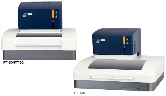
Fig.1 The FT150 series X-ray fluorescence coating thickness gauge.
The FT150 series lineup consists of three models: FT150, FT150L, and FT150h.
The FT150 is equipped with an X-ray irradiation system optimized for measurements of Au/Pd coatings at the 10 nm thickness level. This instrument is positioned to be the successor to Hitachi High-Tech Science's previous model.
The FT150L has a large specimen chamber with the same basic components as the FT150. The large specimen chamber is specialized for measuring large print circuit boards up to 600 mm × 600 mm.
The FT150h is equipped with an X-ray irradiation system having a wide applicable range of X-ray energy. This instrument allows for more general purpose thickness measurements. This is a unique instrument—a type of instrument that was not present in Hitachi High-Tech Science’s previous product lineup—and we expect it will find a wide range of applications in the coming years.
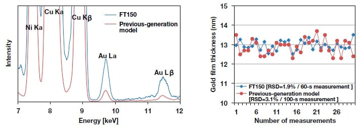
In developing the FT150, we revisited all of the components of the X-ray detection system used in our previous products. As a result, the X-ray detection sensitivity is increased about twice as high as that of our previous model, and measurement time for getting the same precision is reduced almost to half. Figure 2 compares measurement results of a Au(13 nm)/Pd(12 nm)/Ni-coated Cu sample using the FT150 and a previous-generation model. The peaks in the X-ray fluorescence spectrum (left side of figure) obtained using the FT150 (blue) are higher than those obtained using the previous-generation model (red), indicating greater X-ray intensity. Thicknesses obtained from 30 times of repeated measurements of the same sample are plotted on the right side of the figure, from which it can be seen that the results of FT150 exhibit smaller variations than those of the previous machine, though measurement time of FT150 has 40 seconds of advantage.

Fig.2 Comparison of results obtained with FT150 and previous-generation model.
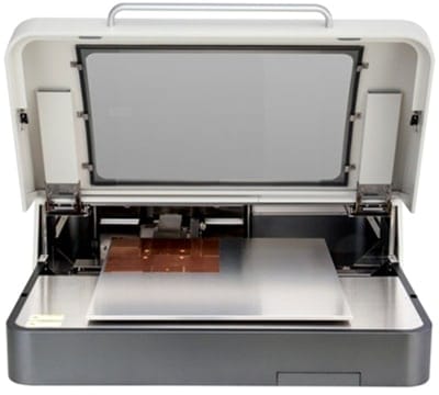
The FT150 is often used in production areas of electronic components or printed circuit boards, not in lab. For these reasons, we have engineered the instrument in ways that not only improve the measurement performance but also reduce the burden on the user regarding matters such as the insertion and removal of samples and alignment of the sample position. For example, when working with large-scale printed circuit boards, if the sample space is narrow, users must carry out highly delicate manipulations to avoid damaging the circuit board to be measured. As shown in Figure 3, the FT150L offers a larger port into the sample chamber and a more generous amount of space above the stage to ensure that users are not obstructed when positioning the sample. Thus, even large, flexible circuit boards that may easily distort may be placed on the stage plate without worry. Moreover, the region to be measured can be brought rapidly into the field of view of microscope for sample observation. In addition, the large observation window allows for visual confirmation of the sample position and the measurement region when the cover is closed. The instrument is equipped with a mechanism to assist in opening and closing the sample chamber, ensuring that users may easily open and close this cover with one hand despite its large size.
Because the FT150 series instruments use high-intensity X-rays, their design includes proper attention to safety considerations. In instruments designed to measure large printed circuit boards, the cover to the sample chamber tends to be large and unwieldy. For this reason, some commercially available models are designed with slits cut into the cover, through which printed circuit boards can be inserted. However, to guarantee that an X-ray based instrument can be used with no fear of safety risks, it is insufficient to merely ensure that there is no need to establish a radiation control area. Rather, it must be designed with no slits or other open ports so that X-ray leakage outside the instrument is minimized. The structure that we have designed, despite the easy-to-open large cover, satisfies this requirement and thus balances safety with ease of use.

Fig.3 The FT150L with its cover opened.
The operating software provided with the FT150 also incorporates a new user interface. The key features of this redesigned software include (a)the new concept of apps, which package commonly executed measurement procedures, (b)a user interface in which required operations are always indicated on the top of the screen, and (c)data management via a database.
Each app packages a variety of information, including analytical conditions, information on measurement positions, and data to be added to the results of measurements.
These apps are displayed as icons within the "Launcher" window displayed when the software is first launched. Users may select any desired image—including graphical images or illustrations indicating the layer structure of a measured object—to serve as the icon for an app, allowing for their easy identification. Routine measurement procedures may be initiated simply by launching the software and clicking the desired icon. Moreover, a measurement navigator serves as an operational guide, displaying information on the current operational procedure that moves together with the measurement window. By reporting the various procedural steps—such as positioning the sample, specifying the measurement position, initiating the measurement, producing output reporting measurement results, and terminating the measurement—users may make measurements with minimum hassle, improving the operational efficiency and reducing procedural errors.
In addition, using the optional touch panel monitor allows users to perform operations more intuitively in the immediate vicinity of the instrument, further enhancing the operational efficiency.
The results of measurements are automatically stored in a database together with associated information, such as the time and date of measurements, analytical conditions, sample images, and X-ray spectra, allowing comprehensive data management. Within the database, it is possible to search for data using information on samples (date, sample name, name of instrument user, etc.). This not only allows desired data to be retrieved with ease, but also facilitates the monitoring of trends in measurement results and the creation of statistical data.

Fig.4 Software GUI.
We have presented a concise discussion of the features of the FT150 series. We have every hope that the ability of these instruments to provide high-precision measurements of the ultraminiature components used in cutting-edge technological devices, together with their outstanding ease of use, will encourage their widespread adoption as coating thickness measurement devices.
Author
*1Haruo Takahashi
Analytical Methods Group
Hitachi High-Tech Science Corporation
See more