Masahiro Kiyohara*1, Takahiro Sato*2, Shota Torikawa*1
FIB-SEM Systems (FIB: Focused Ion Beam; SEM: Scanning Electron Microscope) are widely used as tools for preparing thin samples for analysis by Transmission Electron Microscope (TEM) and other applications. In recent years, the increasing diversity and miniaturization of structures to be analyzed have spurred researchers to conduct higher-precision analyses. This has resulted in a demand for higher-quality sample preparation techniques, including FIB-SEM systems. To realize this objective requires surmounting a number of challenges, including the following:
In this regard, FIB-SEM systems are playing an increasingly important role. At Hitachi High-Tech, we are developing technologies responding to the above issues. Multiple methods for resolving the above challenges are presented in this article by using the TriplebeamR NX2000 FIB-SEM system (Figure 1).
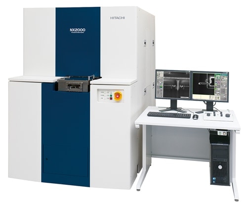
Fig.1 NX2000 instrument
The strategy typically adopted for addressing challenge 1-1 above—by reducing damage due to FIB processing—is to apply low-energy argon ion beam at the fi nal processing stage. With Hitachi High-Tech's system, the exposed cross section can be observed by SEM simultaneously during FIB etching process without sacrifi cing SEM resolution. This enables precise end-point detection at the user defi ned location.
The trend toward miniaturization of structures and the need for higher-precision analysis have increased the demand for higher-quality samples with less surface damage.
As shown in Fig. 2, the Triplebeam® system—a unique instrument configuration developed by Hitachi High-Tech—consists of a Focused Ion Beam (FIB), an Electron Beam (EB), and an argon ion beam (Ar) focusing at one coincidence point;1) the damage layer resulting from FIB processing can be removed by etching with the low-energy Ar ion beam.
The key advantages of the Triplebeam® system include the following:
The design advantages of the Triplebeam® system's approach to address the challenges described in 1-1 and 1-2 can effectively yield superior high quality results.
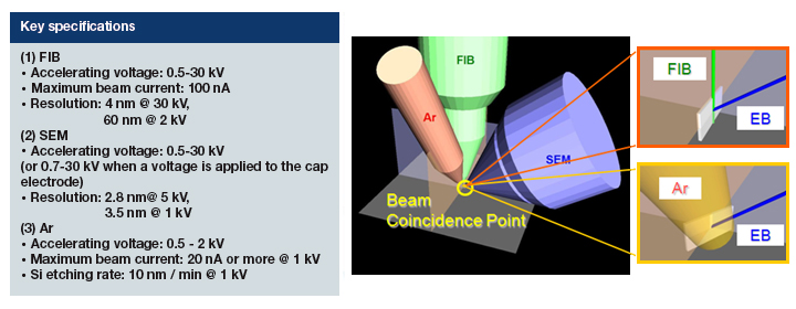
Fig. 2 Key specifications of NX2000 and basic configuration of the Triplebeam® system
The NX2000 system also includes a new option; a Xe ion beam, which has approximately 3.2 times the mass of Ar ions. Similarly to the Ar ion-beam system, the accelerating voltage of the Xe ion beam can be varied over the range of 0.5-2.0 kV. The added fl exibility of the low energy ion system allows for the same system to supply either a Xe ion beam or an Ar ion beam simply by switching the supply gas for the ion source.
Fig. 3 shows TEM images of a GaN sample with fi nal-stage processing conducted with an Ar ion beam and a Xe ion beam2). As is the case for the Ar ion beam, the underlying lattice is clearly visible in the TEM image for the sample using fi nal-stage processing with the Xe ion beam.
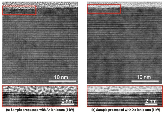
Fig.3 TEM images with two final-stage processing methods.
Sample: Single-crystal GaN
Instrument: HF-3300
Accelerating voltage: 300 kV
To mitigate curtaining effects, Hitachi High-Tech has been involved in the development of Anti-Curtaining Effect (ACE) technology. One component of this technology is a sample-orientation control using microsampling with an axis of rotation, this technique has been widely accepted3). However, in recent years such conventional methods are becoming insuffi cient for most advanced devices with increasing complexity of three-dimensional structures.
To address this diffi culty, we have developed the double-tilt system as a new component for addressing curtaining effects in samples with complex structures typically found in today's cutting-edge high-performance devices.4)
This section describes this new technique.
The double-tilt system consists of a standard 5-axis motorized sample stage which is mounted on a 2-axis tilting mechanism. This results in a motorized sample stage with a total of 7 axes of motion. Although each axis can be controlled independently, we have created a user-friendly software control environment to assist operators when carrying out procedures with the instrument. In addition, the double-tilt system can be mounted or unmounted by operators without breaking the vacuum in the sample chamber. Thus, the instrument can also be used as a conventional 5-axis motorized sample-stage instrument.
The adoption of the double-tilt system allows the change of direction and incidence angle of the incoming ion beam during TEM sample preparation while monitoring by SEM on a real time basis.
Fig. 4 shows a comparison of the preparation results for a 3D NAND fl ash-memory sample with and without the double-tilt system employed. In 3D NAND fl ash memory arrays, there are complex structures consisting of multiple differing materials across a wide area of the cross section. For this reason, there are signifi cant curtaining effects under conventional conditions, as shown in Fig. 4(a). In contrast, the double-tilt system realizes multiple incidence angles during the etching process. This results in a drastic reduction of curtaining effects during sample preparation, as shown in Fig. 4(b).
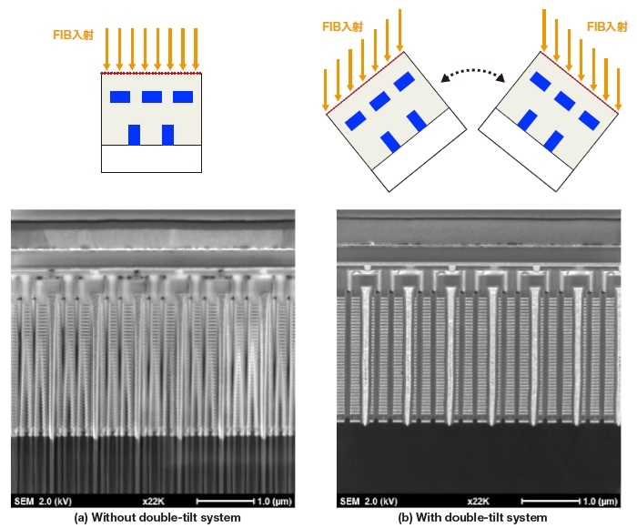
Fig.4 Reduction of curtaining effects using the double-tilt system.
Sample: 3D NAND flash memory
In this article we introduced the Triplebeam® system—a proprietary technology developed by Hitachi High-Tech—as well as two new features of the NX2000: the low-energy Xe ion-beam system and the double-tilt system. On the Triplebeam® system, ACE technology, such as the double-tilt system and low-energy Xe ion-beam processing, enables high-quality sample preparation with higher throughput.
Hitachi High-Tech is committed to meeting the R&D and quality-control needs of researchers and engineers by reducing the burdens associated with sample preparation and building higher-precision analytical technologies.
Notes
References
Author
*1 Masahiro Kiyohara, Shota Torikawa
Beam Technology System Design Department
Design Division
Hitachi High-Tech Science Corporation
*2 Takahiro Sato
Scientific & Medical Systems Business Group
Scientific Systems Product Div, Application Development Dept
Hitachi High-Tech Corporation
See more
