Shigeru Wakiyama
Probe microscopes are instruments that produce images by detecting various kinds of physical interactions between a probe and a sample. The first method of probe microscopy was scanning tunneling microscopy (STM), developed in 1983 at IBM Research - Zurich; this method was used to obtain important atomic-scale images that resolved the question of the structure of the Si(111) 7×7 surface reconstruction. The developers of STM, G. Binnig and H. Rohrer, were awarded the 1986 Nobel Prize in Physics.
STM is a probe microscopy technique that uses a tunneling current. The year 1986 witnessed the development of atomic force microscopy (AFM), which extended the range of probe microscopy to allow observations of the surfaces of non-conductive materials; in the following years this technique was rapidly adopted in surface science and related industrial sectors.
Hitachi High-Tech Science Corporation (formerly Seiko Instruments Inc.) participated in the development project that produced Japan's first successful atomic-scale STM observation—a project supported at that time by Japan's former Ministry of International Trade and Industry, the Agency of Industrial Science and Technology, and the Electrotechnical Laboratory—and in the ensuing years we have continued to develop a variety of related instruments. In this report we introduce the AFM5500M probe microscope, which we have developed to achieve several goals: improving the reliability of measurements to eliminate measurement errors, automating measurements to improve productivity, and enhancing measurement affinity to facilitate linkage with other methods of diagnostic analysis.
Figure 1 is a schematic diagram illustrating the basic principles of AFM measurements. The two most common AFM measurement modes are contact mode and dynamic mode (also known as vibrational mode); our discussion here will consider the case of dynamic mode, the standard mode of usage.
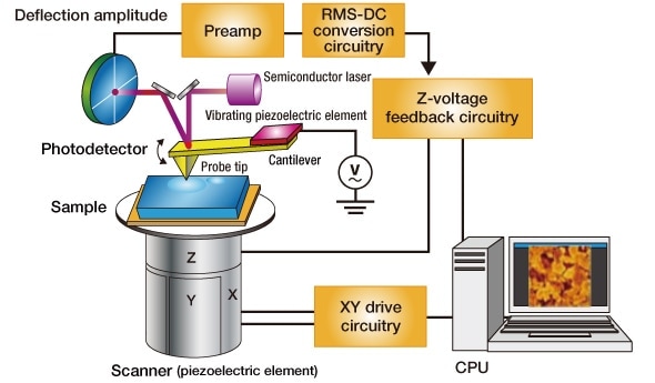
Fig 1. Principles of probe microscopy
A cantilever is positioned facing the measurement sample and a sharp probe tip is formed at the end of this cantilever. Cantilevers are generally made of silicon and produced by microetching. When the cantilever is driven to vibrate at a frequency near its resonance frequency and the probe tip is brought near the sample, the amplitude of the cantilever oscillation changes due to physical forces acting between the tip and the sample. This variation in cantilever amplitude is detected by shining laser light on the rear surface of the cantilever and detecting the reflected light with a photodetector (an optical-lever system); the resulting AC signal is then converted to a DC signal by RMS-DC conversion circuitry.
The sample is mounted atop a scanner capable of ultrafine motion in the in-plane (X,Y) and vertical (Z) directions. The probe tip is brought to within a sufficiently close distance of the sample that the physical forces (including atomic forces and other forces) acting between tip and sample are detectable, and the scanner is then used to scan in the in-plane directions; the cantilever amplitude varies in response to the tip-sample distance—which varies in turn with the surface morphology of the sample—and the scanner is controlled in the vertical direction to maintain the vibration amplitude at a constant value.
Combining the in-plane scanner signal with the vertical control signal then yields a three-dimensional image representing the sample surface morphology.
In general, probe microscopy offers a number of advantages, including high-resolution measurements, the ability to measure different physical quantities using various measurement techniques, and the ability to make measurements in a variety of environments. Figure 2 shows examples of images obtained via probe-microscope observations. The range of sample areas that can be observed is determined by the range of motion of the scanner and typically runs from a few nanometers to a few hundred micrometers.
STM and ATM respectively measure the tunneling current flowing between the tip and sample and the atomic forces acting between the tip and sample; because both quantities depend sensitively on the tip-sample distance, both methods allow high-resolution observations of sample surfaces.
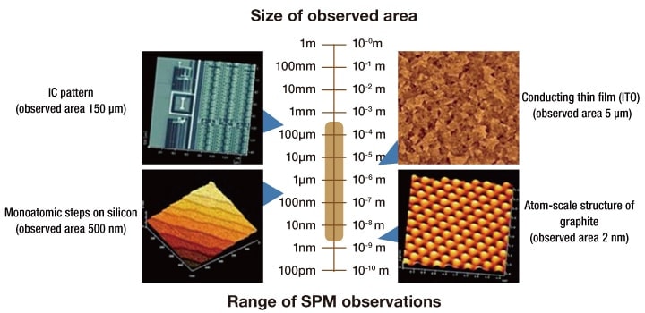
Fig 2. Examples of probe-microscope images
Probe microscopy allows not only measurement of the sample surface morphology, but also simultaneous measurement and observation of various other physical quantities. As shown in Figure 3, multi-functional measurement capability allows measurements of many physical quantities including mechanical properties, thermal properties, electrical properties, and magnetic properties. These instruments may also be used for purposes other than measurement—for example, by exploiting mechanical forces or principles of anode oxidation to accomplish fine-grained processing of sample surfaces.
The mechanical properties that may be measured include friction forces and viscoelasticity of the sample surface. The thermal properties include physical properties associated with the temperature of the sample. Measurements of electrical properties include conductivity mapping, potential mapping of the sample surface, and dopant profile for semiconductors. Magnetic properties include magnetic fields in magnetic materials such as those used in hard disk drives.
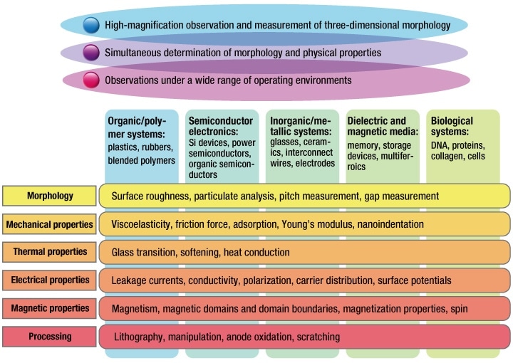
Fig 3. Applications of probe microscopy
Probe microscopy measurements may be performed in many different environments, including not only ambient conditions but also in vacuum, in inert-gas environments, and in solution (assuming the cantilever does not react with the solution in question). For example, pristine sample surfaces may be observed in a vacuum, sample surfaces may be modified by gas injection, or changes in surface morphology due to sample heating or cooling may be observed.
Figure 4 shows photographs of the AFM5500M system: the AFM unit (left) and the soundproof cover (right) with the AFM unit positioned inside and the control unit positioned below. Figure 5 shows a schematic depiction of the AFM5500M system configuration. In this section we discuss the various elements that comprise the AFM5500M.
The AFM5500M is operated using a personal computer on which the results of measurements are displayed. As shown in Figure 5, the control circuitry, XY drive circuitry, Z control circuitry, and other control elements are located inside the control unit. As noted above (‘Advantages of probe microscopy'), probe microscopes are capable in principle of achieving high resolution, but in some cases vibrational noise transmitted from the floor supporting the instrument may contaminate measured image data. To mitigate this problem, AFM units typically are installed on a vibration-isolation mechanism, which may be passively or actively controlled. Passively-controlled systems typically use vibration-isolating springs with resonance frequency on the order of a few Hz, and thus are not useful for reducing low-frequency environmental vibrations. The AFM5500M uses a tabletop actively-controlled vibration isolator that is capable of reducing low-frequency vibrational noise. In some cases, acoustic (sound) noise from the surrounding environment may also contaminate measured image data. To address this noise source, the AFM unit is placed inside a soundproof cover, which consists of multiple layers of metallic plates, sound-blocking sheets, and sound-absorbing sheets. The metallic plates and sound-blocking sheets suppress the transmission of external acoustic noise into the interior of the soundproof cover (mass effect), while the sound-absorbing sheets reduce the effect of echoes within the cover.
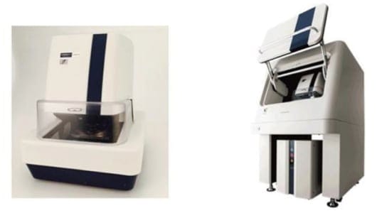
Fig 4. The AFM5500M system. Left: AFM unit. Right: Soundproof cover and control unit

Fig 5. Configuration of the AFM5500M
The sample is mounted on the sample stage. The sample stage is then mounted on an electrically actuated stage that allows observations spanning the full area of samples as large as 4 inches (100 mm). The cantilever is positioned above the sample, as is the optical-lever system consisting of a laser light source and a photodetector that is used to detect the cantilever displacement. Although Figure 1: Principles of probe microscopy considered the possibility of using a scanner to achieve ultra-fine motion of the sample, the AFM5500M in fact uses a different approach, in which the sample is not moved, but instead the cantilever and optical-lever system can be moved in three dimensions, thus allowing observation of an entire 4-inch sample.
In addition, the instrument is equipped with optical microscopy functionality based on a CCD camera, allowing the sample and cantilever to be displayed on a screen. Optical microscopy images are useful for replacing cantilevers and setting the in-plane (XY plane) position of the cantilever over the sample. The positioning of the optical microscopy and optical-lever systems is carefully engineered1) to reduce resolution loss in optical microscopy images. Although not shown in the schematic diagram, the system also includes a vertical (Z-axis) positioning stage to bring the probe tip to within a sufficiently short distance from the sample that physical forces (atomic forces) are detectable. The entire system is mounted on a high-stiffness granite chassis.
As noted above, the AFM5500M was designed with the goals of improving the reliability of measurements to eliminate measurement errors, automating measurements to improve productivity, and enhancing measurement affinity to facilitate linkage with other methods of diagnostic analysis. In this section we discuss each of these items in turn: In Section 5.1 we discuss high-accuracy measurements over wide scan regions, in Section 5.2 we discuss improved ease of operation due to measurement automation, and in Section 5.3 we discuss measurement affinity with other measurement instruments.
In conventional scanning-probe microscopes, scanning in the X, Y, and Z directions is achieved through the use of a hollow cylindrical piezoelectric scanner such as that shown in Figure 6. Such a scanner is made of a piezoelectric material that becomes distorted when a voltage is applied to it. The hollow cylindrical scan tube is equipped with one inner electrode and one outer electrode divided into 5 sectors: one for Z-scanning motion and two each for X- and Y-scanning motion. Applying voltages to each electrode with respect to the reference (ground) inner electrode causes the scan tube to distort. Application of a negative voltage to the outer electrode causes compression in the thickness direction, causing the scan tube to elongate in the axial direction. Contrarily, application of a positive voltage to the outer electrode causes an expansion in the thickness direction and a compression in the axial direction. By the same principles, applying a voltage to the Z-scan electrode causes a displacement of the scan tube in the Z direction. Scanning in the X direction is achieved by applying voltages of +V to one scan electrode and -V to the opposite scan electrode, inducing a bending motion in the hollow cylindrical tube; scanning in the Y direction proceeds similarly. If the thickness of the piezoelectric tube walls is not uniform, crosstalk arises between the vertical (Z-directed) and in-plane motion of the scan tube. In addition, because the lateral (XY-plane) scanning motion of the probe tip is achieved through the bending motion of the scan tube, curvature effects give rise to a distortion of planarity in the resulting images. This phenomenon leads to errors in measurements of flat samples. Moreover, to enable scanning over wide areas the scan tube must be long, which reduces the stiffness of the materials comprising the scanner unit.
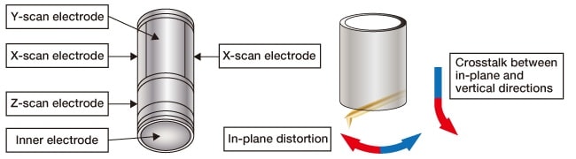
Fig 6. A hollow piezoelectric cylinder and its scan trajectory
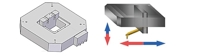
Fig 7. The flat scanner and its scan trajectory
To eliminate effects like this, the AFM5500M adopts a three-dimensional fine-grained actuation mechanism in which the Z-direction motion is separated from the XY-plane motion and a flat scanner (Figure 7) is used to achieve wide-area scanning (200 µm in-plane and 15 µm vertical) while reducing distortion due to the scanner. Also, as noted above in Figure 5: Configuration of the AFM5500M, by placing a low-noise optical position sensor in the vicinity of the cantilever, we improve the accuracy of in-plane (XY) scanning and closed-loop control as well as the detection accuracy in the vertical (Z) direction; this also reduces measurement errors for flat samples arising from the structure of the scanner.
Probe microscopy requires expert preparation and configuration of parameter settings before measurements can be made; in the past, this created the impression that probe microscopes were test instruments of interest to only a small number of researchers with specialized knowledge and training.
The AFM5500M aspires to automate much of the measurement process to improve ease of use and eliminate measurement errors caused by users. In this section—referring to the Figure 8: The procedural flow leading to an AFM5500M measurement—we give a detailed explanation of the procedural flow leading up to an AFM5500M measurement.
The AFM5500M uses a three-dimensional cantilever scanning technique. This requires a preparatory procedure in which a cantilever is affixed to the cantilever mounting block at the tip of the scanner. Cantilevers are typically fabricated by silicon processing and have dimensions on the order of 10 µm (width) × few 100 µm (length), so attempts to install cantilevers by hand would both complicate the use of the instrument and degrade the reliability of measurements. The AFM5500M is equipped with automatic cantilever replacement functionality that solves this problem.
The cantilever is held fixed inside a cartridge (Figure 8, 1-1) whose surfaces are coated with weakly adhesive gel. At this point the cartridge is placed on a block atop an electrically actuated stage that moves in the X and Y directions (Figure 8, 1-2). The cantilever may be supplied with a pre-mounted configuration, as in Figure 8 1-1, or alternatively the cantilever alone may be supplied. In the latter case, a special tool is used to fix the cantilever in the cartridge. The cantilever cartridge may hold up to five cantilevers. By selecting which of these cantilevers to use (Figure 8, 1-3), the XY stage may be used to position the cantilever cartridge at a point with specified coordinates. Then the Z-axis stage descends to a position from which the laser spot of the optical lever and the outline of the cantilever are visible using the optical microscope.
The laser spot and the outline of the cantilever can be seen through the optical microscope, so image-recognition techniques are used to adjust the position of the cantilever and the center of the laser spot via an electrically actuated stage capable of motion in the X and Y directions (Figure 8, 2-1). Next, the Z-axis position is electrically decreased until the cantilever comes into contact with the mounting block at the tip of the scanner. When this happens, the vacuum suction functionality of the mounting block fixes the cantilever in place. With the cantilever thus maintained in position via vacuum suction, the Z-axis stage is raised, completing the handoff to the cantilever mounting block. Laser light impinging on the rear surface of the cantilever is reflected into a four-segment photodetector. The position of the reflected light entering the photodetector differs depending on the size and type of the cantilever, but the signal components from each of the four photodetector segments can be used to compute this position, and the position is then automatically adjusted using a two-axis stage on the photodetector side (Figure 8, 2-2).
The above procedure ensures that the cantilever mounting process, and proper positioning of the photodetector to allow detection of laser light reflected from the rear cantilever surface, are handled automatically by the instrument.
For measurements in dynamic mode (vibrational mode), a Q-curve for the selected cantilever is acquired (Figure 8, 3) and quantities such as the resonance frequency and vibration amplitude are computed. This completes the process of preparing the cantilever; the entire sequence of steps 1–3 is carried out automatically by the AFM5500M.
The XY stage is moved to the sample exchange point and the sample is mounted on the sample stage (Figure 8, 4-1). Vacuum suction may be used to cause the sample to adhere to the stage.
Next, the XY and Z-axis stages are moved and the measurement location is configured by referring to optical microscopy images (Figure 8, 4-2). If an alignment-mark mechanism has been used to define the position of the probe tip on the end of the cantilever, the center of the AFM image can be aligned with the center of the optical microscopy image to within a tolerance of approximately 10 µm; this is sufficient to ensure that the sample region measured by AFM is indeed the region selected via optical microscopy.
Simply selecting automatic parameter-adjustment mode (Item 5 in Figure 8) and clicking the Start button initiates the approach to the target region and the automated adjustment of measurement conditions; there is no need for the user to adjust any parameters. The user need only specify the extent of the region (maximum 200 µm) to be scanned to produce the image; then, based on the shape of the region and the state of the surface, parameters such as the measurement frequency and control gain are adjusted, and the measurement is performed automatically.
As noted above, this automated parameter-adjustment mode eliminates the need for instrument operators to adjust measurement conditions—a task that has conventionally required expert knowledge—increasing the ease of operating the probe microscope and eliminating measurement inaccuracies due to user error.
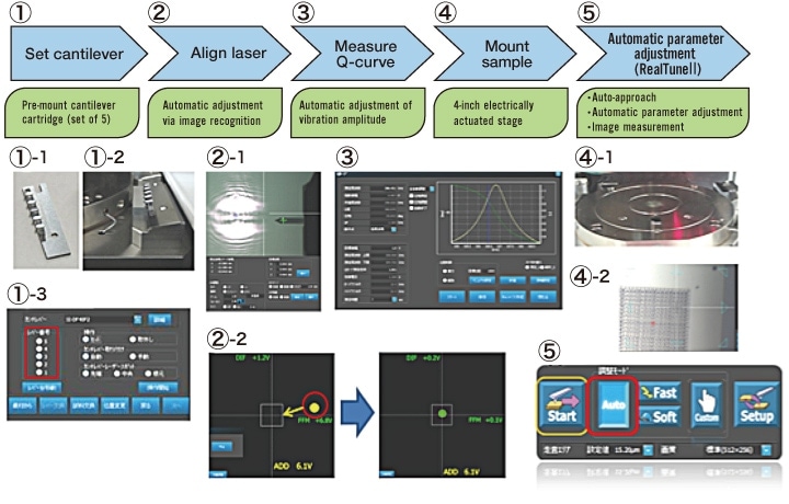
Fig 8. The procedural flow leading to an AFM5500M measurement
There are many types of instruments beside probe microscopes for analysis and measurement of surface morphology, with scanning electron microscopy (SEM) systems being one typical example. The greatest strength of probe microscopes is their ability to furnish realistic height information at high resolution. However, SEM offers the advantages of wide-area measurements, and can be combined with other analytic techniques to carry out component analysis and other types of measurements. By performing measurements using multiple instruments, insights can be obtained that could not be acquired using any one single instrument. With these objectives in mind, we have designed a framework to facilitate linkage of the AFM5500M with two other types of instrument sold by Hitachi High-Tech: our coherence scanning interferometry (CSI) and scanning electron microscopy (SEM) systems (Figure 9). To facilitate this, all instruments share a single common sample stage equipped with alignment marks. The position of these marks, together with measurement positioning data, define coordinate transformations for the stage when mounted in each instrument. This allows all instruments to perform measurements in the same sample region.
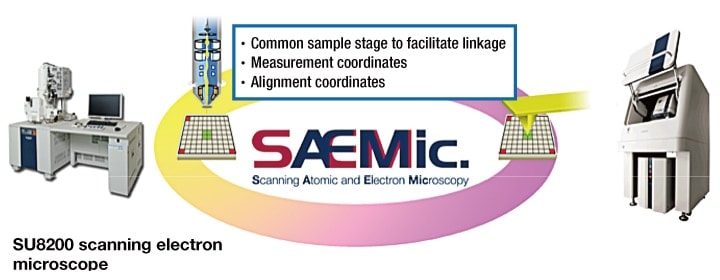
Fig 9. Measurement affinity
Figure 10 shows measurement results for a silicon substrate patterned with features with a height of 100 nm and a pitch of 20 µm obtained using the AFM5500M. The image correctly reproduces the square lattice pattern without any distortion over a wide scan region of 200 µm × 200 µm.

Fig 10. Patterned sample (200 µm × 200 µm)
Figure 11 shows measurement results demonstrating the performance of the flat scanner. Here we are measuring height differences in an amorphous silicon thin film on a silicon substrate. Whereas the image obtained with a conventional instrument (left) exhibits curvature errors due to the structure of the conventional scanner, the imaged obtained with the AFM5500M (right) exhibits good planarity over a wide sample region of length 200 µm, as noted above in our discussion of the AFM5500M's key features.

Fig 11. Improved measurement accuracy (1): reduction of in-plane distortion due to flat scanner
Figure 12 shows a second example demonstrating the regularity of the AFM5500M scanner; here we measured a textured structure in a photovoltaic cell (PVC) using both the AFM5500M and a conventional instrument. Due to the poor z-axis regularity of the conventional scanner (a hollow piezoelectric cylinder), left-right asymmetry is present in the triangular cross-sectional profile of the textured structure. In contrast, the AFM5500M yields a more accurate measurement of the three-dimensional structure, reflecting the left-right symmetry arising from the crystal orientation.

Fig 12. Improved measurement accuracy (2): reduction of crosstalk between in-plane and vertical directions
Figure 13 presents an example of measurement affinity in which AFM and SEM were used to observe the same region of a single-phase graphene/SiO2 sample fabricated by chemical vapor deposition (CVD). To investigate the source of the contrast present in the SEM image, we overlaid AFM-captured morphology images and electric-potential images on the SEM image. From the superposed images it can be seen that the contrast difference in the SEM image corresponds to the height of a single graphene layer as determined by scanning probe microscopy, and moreover that the surface potential depends on the number of graphene layers and other factors.2)
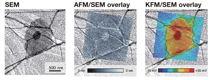
Fig 13. An example of measurement affinity between AFM and SEM
Figure 14 illustrates measurement automation enabled by automatic adjustment of measurement parameters. With a single click of the Start button in Auto mode, the feedback gain and other measurement parameters are chosen automatically from the Q-curve adjustments.
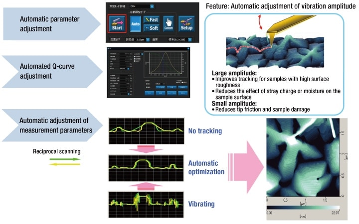
Figure 14. Automatic parameter adjustment
In this report, after introducing the operating principles and metrological applications of probe microscopes as instruments for observing and measuring sample surfaces, we discussed the design and features of the AFM5500M—an instrument developed with the specific goal of improving measurement reliability—and presented sample applications illustrating its use. By automating the measurement process, this instrument reduces the need for users to be experts in operating probe microscopes, thereby reducing or eliminating measurement errors attributable to users. Moreover, the AFM5500M retains the key strengths of probe microscopes, such as three-dimensional data acquisition and the ability to perform multiple types of measurements. It also offers increased interoperability with other instruments, paving the way for an expansion of probe microscopy techniques in combination with other metrology solutions.
To date, one drawback of probe microscopy has been the relatively long measurement times required compared to other measurement techniques. However, given the ongoing active effort to accelerate the speed of probe microscopes, we are hopeful that these instruments will prove increasingly ubiquitous tools for surface testing in the future.
References
Publication data
Published in the monthly journal Engineering Materials (March issue 2017)
Authors
Shigeru Wakiyama
Beam Technology Systems Design Department
Hitachi High-Tech Science Corporation
See more
