Hiroyuki Ito*1, Yuki Inagi*2
Ion milling systems are widely used as instruments for preparing cross-section samples for scanning electron microscope (SEM), with applications to fields such as materials science and semiconductor research. The two types of ion-milling methods commonly used for SEM samples are flat milling and cross-section milling1), and Hitachi High-Tech develops and sells both types of instrument. The increasingly complex structures of the samples observed via SEM—in fields such as semiconductors, electrical and electronic components, and soft materials—is changing the nature of the demand for ion milling systems. In particular, demand has grown for machines offering reduced milling times, and cross-section milling rates have increased more than tenfold over the past ten years(*1).
In this article, after first reviewing the basic principles of ion milling, we will discuss the features and advantages of Hitachi's latest ion milling systems and present a number of case studies demonstrating applications of ion-milling processing.
Ion milling uses the phenomenon of sputtering2)—in which atoms are ejected from a sample surface irradiated by ions accelerated by an electric field—to produce millimeter-order smooth surfaces for observation. The ionic material used is typically argon gas, which induces minimal chemical transformation for most sample compositions.
As shown in Figure 1, cross-section milling proceeds by placing a mask between the ion gun and the sample, and then extending a portion of the sample beyond the mask to expose the sample to irradiation from the ion beam. By subjecting the sample portion protruding beyond the mask edge to sputtering along the mask edge, one obtains a flat surface. The extent of the sample protrusion from the mask edge may be set between a few 10s of microns to 100 microns, and by rotating the sample holder over an angular range of ±15 - 40°, one reduces the formation of ion milling defects. In general, cross-section milling techniques are used for samples for which mechanical polishing is difficult, such as bulk samples or samples with multilayer structures.
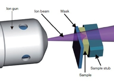
Fig. 1 Schematic diagram illustrating cross-section milling
As an example of cross-section milling, we present a case study involving thermal paper. Figure 2 shows SEM images of pieces of thermal paper after cutting with a razor blade (a) and after cross-section milling (b). When the paper is cut with a razor blade, the stress of contact with the teeth of the blade causes the various layers in the sample to collapse, whereupon it is difficult to discern the layers in the image. In contrast, cross-section milling allows the cross section to be exposed with no application of external stress, avoiding the collapse of layers and allowing the layer structure and thickness to be observed.
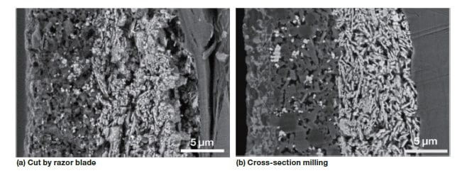
Fig. 2 Cross-section SEM image of thermal paper
Figure 3 shows a schematic view of flat milling. In flat milling methods, an argon ion beam impinges on the sample surface at an angle and the axis of the beam is deflected from the sample rotation axis to allow processing of a wide sample area3). The incident angle θ of the argon ion beam may be varied over the range 0° - 90°4). If θ is set equal to or higher than 80°, the ion beam is nearly parallel to the sample surface, yielding processed surfaces with reduced surface roughness due to differences in etching rate for different crystal orientations and material compositions. This is frequently used for the purpose of final-stage processing with the objective of removing polishing defects that remain after mechanical polishing of resin-embedded samples. Alternatively, by setting θ to low values can take advantage of differences in etching rates to process surfaces in ways that enhance bumps and trenches, which may be used for purposes such as distinguishing the layers of multilayered films.
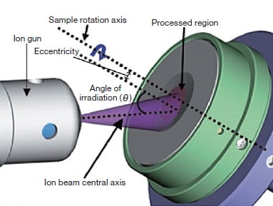
Fig. 3 Schematic diagram illustrating flat milling
Figure 4 shows SEM images of a resin-embedded steel sample after mechanical polishing (a) and after subsequent flat milling (b). Because the mechanical polishing alone does not adequately cleanse the sample surface, it difficult to observe crystal grains in this state; however, with flat milling it is possible to remove the detritus of the polishing procedure and eliminate any defects it creates, revealing crystal grains with full clarity.
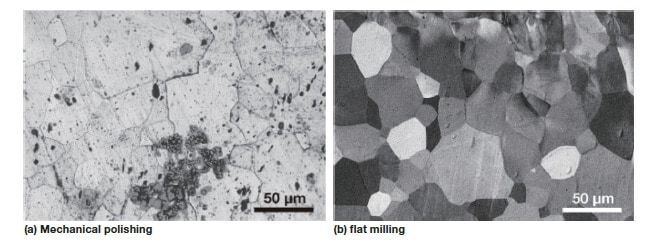
Fig. 4 Example of flat milling of steel material
Hitachi High-Tech has been developing and selling ion milling systems for electron-microscope samples since 1985. In this article, we present the two most advanced instruments available today.
The IM4000PLUS is a hybrid ion milling system offering both of the two capabilities discussed above: cross-section milling and flat milling. The wide variety of applications this instrument supports, together with its extensive lineup of optional accessories—including an air protection milling holder for analysis of lithium-ion battery materials and a sample-cooling system to reduce thermal damage to resins and polymer materials caused by beam irradiation—have made this instrument a huge hit in the marketplace. Moreover, in response to requests for shorter milling times, we have equipped the IM4000PLUS with a high-rate ion gun capable of cross-section milling rates in excess of 500 µm/hour(*2). Figure 5 shows the IM4000PLUS as configured with various optional accessories.
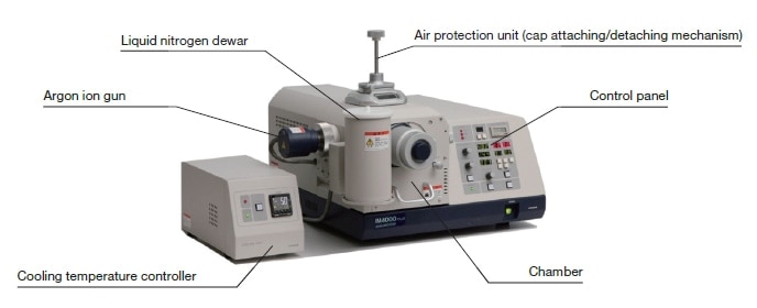
Fig. 5 The Hitachi IM4000PLUS ion milling system equipped with various optional features
(The instrument shown is equipped with the air protection unit and the sample-cooling temperature control unit.)
To cool samples, the IM4000PLUS uses an indirect cooling method in which the vicinity of the sample is cooled by a mesh of copper wires in contact with a dewar filled with liquid nitrogen. This indirect cooling suffices to ensure that resinous or rubber-based materials remain below their glass transition temperature; to prevent overcooling, we have added a heater to allow the temperature to be controlled over the range 0-100°C. Figure 6 shows SEM images of a silicone rubber sample after cross-section milling at room temperature (a) and under cooled conditions (b). Note the presence of wrinkles in the room-temperature cross-section milled sample in regions where the rubber parent material is present; these are due to the increased temperatures produced by argon ion beam irradiation. In contrast, the wrinkles are greatly reduced in the cold-milled sample, indicating a reduction in sample heating.
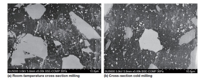
Fig. 6 Example of cross-section milling of silicone rubber
We developed the air protection cross-section milling holder for use with lithium-ion battery materials, whose shapes suffer significant distortion upon reacting with oxygen and water in the atmosphere. The holder features a screw-on cap which may be closed tightly to allow SEM observation after ion milling without exposing the sample to the environment. For reference, we describe here the operating procedure for air protection cross-section milling.
Figure 7 shows SEM images of a lithium-ion battery anode material as processed by air protection cross-section milling (a) and—to confirm the importance of environment isolation—after exposure to the environment for about 10 minutes (b). Whereas the layered graphite structure is clearly visible in Figure (a), in Figure (b) the contact with environmental oxygen and water has produced sedimentary deposits in all regions of the anode material cross section, thus demonstrating the usefulness of the air protection milling holder.
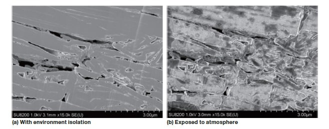
Fig. 7 Example of cross-section milling of a lithium-ion battery anode material
Thus we see that the IM4000PLUS is Hitachi's standard-model ion milling system with support for a wide variety of applications and optional additions for sample cooling and air protection milling.
Pictured in Figure 8, the ArBlade5000 was developed—as its name suggests—to prepare cross-section samples by rapid cutting with argon ions serving as a blade. This instrument, released in April 2017 as a higher-end version of the IM4000PLUS, is equipped with the popular hybrid ion milling capability of its predecessor, allowing both cross-section and flat milling.
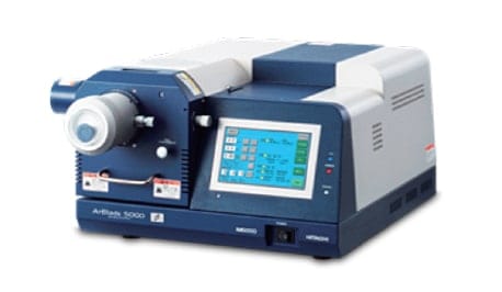
Fig. 8 The ArBlade5000
The ArBlade5000 is equipped with a newly developed high-milling-rate ion gun (the Plus II Ion Gun) and boasts a cross-section milling rate of ≥1 mm/hr (for an accelerating voltage of 8 kV with a silicon sample and protrusion of 100 µm from the mask), more than twice the rate of the IM4000PLUS. With this instrument, cross-section samples may be prepared in a short time even for materials with low sputtering yield(*3), which otherwise require milling for long periods of time. In conjunction with the increased rate of the ion gun, we have also added the SH Mask as a new mask for cross-section milling of materials with low sputtering yield. The SH Mask offers higher ion-beam resistance than conventional pure-Ti mask, making it useful for long-duration cross-section milling. The SH Mask is made of WC (tungsten carbide), a material that does not contain cobalt.
Figure 9 shows the results of cross-section milling of mechanical pencil lead (hardness 4H) for 90 minutes with the IM4000PLUS (a) and with the ArBlade5000 (b). Mechanical pencil lead is composed primarily of carbon in the form of graphite, a material whose low sputtering yield makes it difficult to remove via ion milling. As seen in the images, whereas the IM4000PLUS processes only the upper half of the pencil-lead sample, the higher milling rate of the ArBlade5000 allows processing of the entire sample.
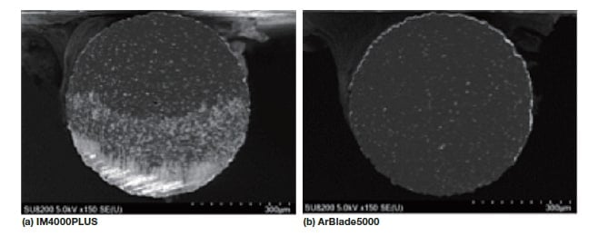
Fig. 9 Comparison of cross-section milling results for mechanical pencil lead (hardness: 4H)
The ArBlade5000 also comes standard equipped with new wide-area cross-section milling capabilities. Whereas conventional cross-section milling techniques are restricted to processing sample regions of roughly 1 mm in width, the ArBlade5000 can process up to a maximum width of 8 mm. Figure 10 shows the results of processing an electronic circuit board using this wide-area milling capability. Figures (a) and (b) show the entirety of the processed surface and an enlargement of the region of contact between an electrode and solder, while (c) shows an EDX mapping image of the enlarged region. The dashed yellow line in the whole image of (a) shows the region that was processed by ion milling; its dimensions are approximately 7 mm(width) by 1 mm(depth). The time required for cross-section milling in this case was 5 hours, demonstrating the ability of the ArBlade5000 and its Plus II Ion Gun to produce large cross-section milled surfaces in short periods of time. In the enlarged image (backscattered-electron image) and the EDX map of the electrode/solder contact surface, one clearly sees layers of copper/tin alloy and other elements of the material composition distribution characteristic of this surface; this demonstrates the possibility of obtaining milled surfaces satisfying the requirements for high-resolution SEM observation and EDX analysis.
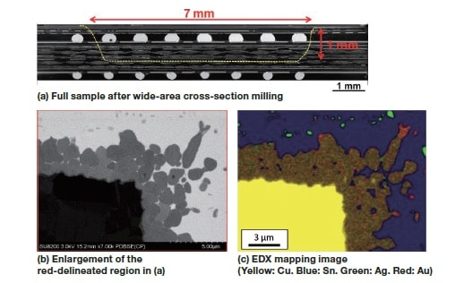
Fig. 10 Example of wide-area milling of an electronic circuit board
In addition, for the ArBlade5000 control panel we adopted a liquid-crystal display touch-panel, and we equipped the instrument with features to reduce the operational burden placed on users, including a timer (offering the ability to set the time remaining before the start of milling) and 2nd-milling functionality (a function that allows two types of processing to be programmed, after which the operation is executed automatically). Whereas the IM4000PLUS uses rotary dials to set the accelerating voltage and the discharge voltage, the ArBlade5000 allows these quantities to be set in 0.1 kV steps, facilitating highly detailed specifications of the milling conditions.
To summarize, the ArBlade5000 is the high-end model in Hitachi's ion milling system lineup; the dramatic increase in milling rate that it offers, together with the ability to process large sample regions with sizes on the order of millimeters, makes it particularly valuable for studies of electronic components, metallic components, and other related areas in which ion-milling machines are in high demand.
Thus far, we have discussed the use of ion milling systems for processing SEM samples, the primary application for these instruments. In this final section we present a case study in which ion milling was used to prepare a sample of a lithium-ion battery material for observation via atomic force microscope (AFM)6). In this case we use ion milling methods to prepare AFM samples for scanning spread resistance microscopy (SSRM) to study changes in the internal electrical resistance of a cathode material for a lithium-ion battery. Figure 11 shows, for a cross-section sample of a lithium-ion battery cathode prepared by cross-section milling, an SEM image (a), an enlargement of this image (b), and an SSRM image of the region observed in (b). The SSRM image allows clear observation of the difference in electrical resistance between the active substance and the conducting metal foil. Moreover, from the unusual contrast regions (high-brightness regions) observed in image (b), we conclude that the region has low resistance. This demonstrates that cross-section milling is useful for preparing AFM samples as well as SEM samples.
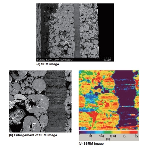
Fig. 11 Results of cross-section SEM-AFM observations of a cathode material for lithium-ion batteries
In this article, we described the features and functionality of the latest ion milling systems and presented a number of case studies. In particular, ion milling rates have increased tenfold over the past 10 years, yielding a dramatic reduction in the time required for ion milling processing. Moreover, features such as cold milling, wide-area cross-section milling, and air protection milling have extended the range of applications to AFM and other areas. In the future, we hope to contribute to the advancement of all varieties of metrology and structural analysis by developing instruments that meet the needs of our users.
References
Publication data
Published in the monthly journal Engineering Materials (November issue 2017)
About the authors
*1 Hiroyuki Ito
Marketing Department
Science Systems Sales & Marketing Division
Science & Medical Systems Business Group
Hitachi High-Tech Corporation
*2 Yuki Inagi
Application Development Department
Science Systems Product Division
Science & Medical Systems Business Group
Hitachi High-Tech Corporation
See more