Yusuke Ominami*1, Takeshi Kamimura*2, Kota Takagi*2
The scanning electron microscope (SEM) is widely used in electronics, biotechnology, materials engineering, and nearly every other industrial sector as an instrument for observing the fine-grained structure of the surfaces of material bodies. Historically, SEMs were extremely large instruments, but in 2005 we released the Miniscope® TM-1000 as the first realization of an innovative new paradigm: an SEM that anybody can use. TM series instruments earned high praise for their miniature footprint, low price, and ease of use, and to date over 3,500 have been sold (as of December 2016).
When the Miniscope® TM-1000 was released in 2005, we anticipated that the instrument would find use in schools and other educational institutions. Over the following years, however, as we delivered TM-1000 and TM-3000 series instruments to users in a wide range of fields around the world, we became aware of increasing interest in the use of Miniscope® for component testing and other industrial applications. Indeed, the fact that these instruments can be easily installed at component manufacturing sites, and that they allow anyone to capture SEM images with ease—no special skills or training required—makes them highly promising tools for finer-grained testing for impurities and defects and more detailed measurements of manufactured components.
Motivated by this background, we have now developed the TM4000, a next-generation tabletop microscope that aspires to meet the needs of users who rely on SEM observations for routine operations—such as component testing at manufacturing sites for industrial applications—while retaining the straightforward ease of operation needed for educational applications. In this report, we discuss the key features of the newly developed TM4000 series and present illustrative examples of practical applications.
Figure 1 shows the TM4000. Like previous instruments in the TM series, the TM4000 is a low-vacuum SEM with a thermal electron gun that seeks to achieve a lightweight, miniature footprint and to streamline operating procedures so thoroughly that even first-time SEM users can make observations with no difficulty. The TM4000 also boasts several innovative new features that set the instrument apart from its predecessors, including the new SEM-MAP navigation feature—which allows users to navigate samples using images captured under vacuum conditions by a camera mounted inside the vacuum sample chamber, moving to the desired observation region with a single click of a mouse—and (standard) report-creation software that allows the creation of observed-image reports after the completion of an observation session.
In addition, compared to previous-generation models in the TM3000 series, the TM4000 offers a number of improvements in basic performance, including improved resolution, higher accelerating voltage, a higher-precision sample stage, and a reduction in the weight of the instrument. Instruments in the TM4000 series are also standard equipped with semiconductor backscattered-electron detectors, while the TM4000Plus is additionally equipped with high-sensitivity low-vacuum secondary-electron detector (UVD), allowing acquisition of many types of information on sample morphologies. Instruments in the TM4000 series not only offer enhancements in operational convenience—including camera images taken as the sample is mounted in the instrument, as well as the SEM-MAP mechanism for locating sample regions to be observed—but also improvements in basic performance and report-creation functionality, promising a new level of efficiency in every aspect of SEM operation.
In what follows, we offer detailed discussions of the enhanced operational convenience, improved performance, and report-creation functionality offered by the TM4000 series.
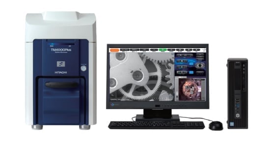
Fig. 1 The TM4000 of tabletop microscope
Figure 2 shows the TM4000 operation window. Like previous-generation models in the TM3000 series, the TM4000 allows observation of images via mouse click and drag operations, and its main window has been enlarged to 1920×1080 pixels. In addition, several items of interest may be viewed in subwindows: images captured by a camera mounted in the vacuum sample chamber, a thumbnail-view list of captured images, images currently being acquired via other detectors, and the SEM-MAP.
The SEM-MAP feature records the position of the sample stage at the time of observation, enabling navigation features such as returning to the position of a captured image or checking the site of the current location within the sample as a whole. In conventional SEM observations, the large sizes of samples caused the currently observed location or previously observed locations to be lost. The SEM-MAP feature significantly improves the operational ease of searching for sample regions to observe.
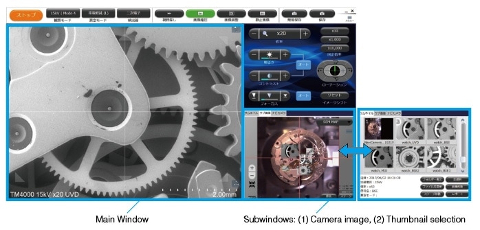
Fig. 2 The TM4000 operation window
Compared to previous-generation instruments, the TM4000 supports samples of sizes as large as 80 mm in diameter and 50 mm in thickness. A newly designed electron optical system yields improved image quality. The new design particularly improves the quality of images obtained at a low accelerating voltage of 5 kV to observe the morphology of sample surfaces (Figure 3). In addition, to meet the needs of both expert and non-expert users, we have added a 10 kV accelerating-voltage mode and a selection of 4 types of probe currents.
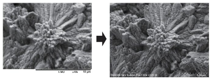
Fig. 3 Improved detail in observed images
Instruments in the TM4000 series come standard equipped with report-creation software that allows users to create reports in Microsoft Word®, Excel®, or Powerpoint® format simply by selecting a template and a captured image. This makes it easier to organize and work with acquired images and other data. Figure 4 shows the TM4000's report-creation window and an example of a report file created with this new feature.
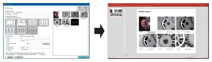
Fig. 4 The report-creation software window (left) and an example of a Powerpoint® report created by this feature (right).
The TM4000Plus captures both backscattered-electron images—which contain information on sample composition in the form of image contrast—and secondary-electron images, which contain information on the roughness of the sample surface. (The TM4000 detects only backscattered-electron images.) Figure 5 shows an image of a sample of adhesive-backed notepaper (a sticky note). Because the observation can be made under low-vacuum conditions, it is possible to observe samples containing water or oils. Moreover, there is no need for metal coatings or other preprocessing steps. Indeed, when performing elemental analysis, secondary-electron images may be acquired with no preprocessing (no metal coating), even for non-conducting materials unaffected by metallic coating materials.
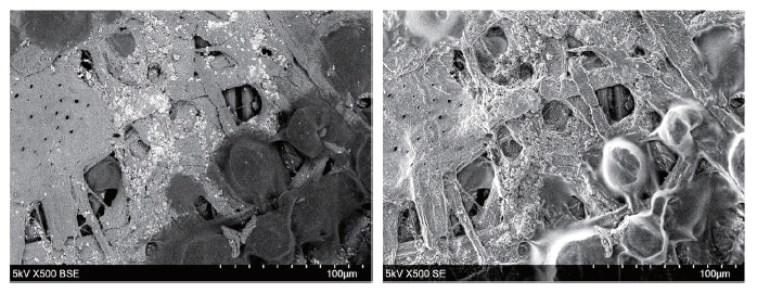
Fig. 5 Observation of a sticky note. Left: backscattered-electron image. Right: Secondary-electron image.
The many user-configurable settings offered by the TM4000—including 3 accelerating-voltage levels, 4 current-mode levels, 2 vacuum-strength settings (3 for the TM4000Plus), and 2 detectors for 3 imaging modes (backscattered-electron imaging, secondary-electron imaging, and mixed imaging)—allow a wide range of types of samples to be observed under customized conditions optimized for the state of the sample and the objective of the observation, as shown in Figure 6.
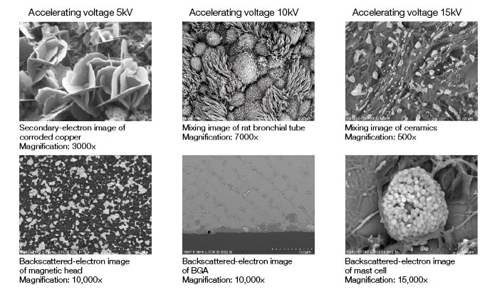
Fig. 6 Images acquired by the TM4000
Instruments in the TM4000 series may be equipped with an optional elemental analysis unit (an energy dispersive X-ray spectroscope (EDS)) to allow elemental analysis of samples under observation. Figure 7 shows an elemental-analysis mapping image obtained for a sample of a clock gear. Distributions of Au, Al, and Ni are clearly visible. In addition to creating elemental analysis mapping images, the analyzer can also display spectra obtained from point or line analyses, allowing users to design a customized data-acquisition portfolio appropriate for the particular sample under observation.
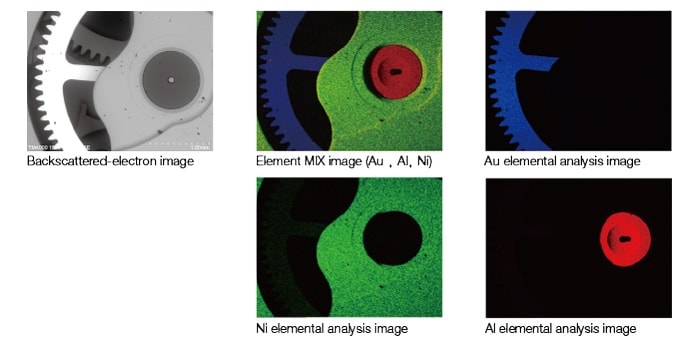
Fig. 7 Elemental analysis images acquired by a TM4000 instrument equipped with an EDS
We have developed the TM4000 series—a line of new tabletop microscopes with a broad range of applications in electronics, biotechnology, materials science, and many other fields. The instruments in this series retain the convenience and compact designs of their predecessors, while offering improvements in functions, operability, and other areas. The innovative new features of the TM4000 series—including the ability to capture camera images under vacuum conditions and report-creation software that prepares observation image reports after an observation has completed—make it a promising new tool for industrial research and other areas of science and technology.
Publication data
Published in the monthly journal Engineering Materials (February issue 2018) (Japanese)
About the authors
*1 Yusuke Ominami
Scientific Systems Business Development Department
Science & Medical Systems Business Group
Hitachi High-Tech Corporation
*2 Takeshi Kamimura, Kota Takagi
Marketing Department
Science & Medical Systems Business Group
Hitachi High-Tech Corporation
See more
