Shigeaki Tachibana
The ability of a scanning electron microscope (SEM) to acquire multiple types of signals such as secondary electron, backscattered electron, and X-ray signals—makes the SEM a flexible instrument that can be used for many different purposes in many different fields of research.
The improved performance and expanded functional range of modern SEMs deliver the advantage of allowing acquisition of many different types of data, but also make the instruments more complicated to operate and increase the time for data acquisition.
The Schottky FE-SEM SU7000, announced by Hitachi High-Tech Corporation in July 2018, is an instrument specifically designed to address these issues; it incorporates new designs for both the electron-optics and detection system to facilitate high-performance measurements with improved throughput.
In addition, to support dynamic observation and measurement—including in-situ observation, an approach that has been an increasing focus of attention in recent years—the instrument is equipped with a specimen chamber and a specimen stage to allow a wide variety of specimen and accessories to be mounted; it is a machine built specifically to support the increasingly diverse range of observation and measurement techniques in use today.
(1) The instrument uses an electron gun equipped with a Schottky emitter, allowing:
(2) Secondary-electron images, backscattered-electron images, and EDX measurements may all be acquired with a single working distance (WD) (6 mm).
(3) Large specimen chamber / specimen stage capable of mounting specimens of dimensions up to 200 mm diameter (horizontal) × 80 mm (vertical) and weight up to 2 kg (including specimen holder)
(4) Display system capable of simultaneously displaying and saving up to 6 signal channels from 5 detectors.
The electron source is equipped with a Schottky emitter. In addition to capturing high-resolution images, the high beam current makes the instrument a good choice for applications such as high-current EDX analysis and high-speed EBSD measurements. Similarly, the instrument offers a relatively large amount of flexibility regarding the vacuum, and is thus well-suited for observations and measurements under low-vacuum conditions.
A two-stage condenser lens allows the probe current to be adjusted from a few pA to 200 nA.
For the objective lens, the instrument uses an assembly consisting of a conical lens (out-lens), of the type commonly used in tungsten SEMs, combined with an electrostatic field (Figure 1).
The effect of chromatic aberration may be listed among the factors responsible for reduced resolution at low accelerating voltages.
Chromatic aberration is caused by the energy spread of the electron beam impinging on the objective lens. The effect is more pronounced for higher values of the ratio ΔE/E, where ΔE is the energy spread of the emitter and E is the primary energy, and is thus especially prominent in observations at low accelerating voltage.
In the SU7000 optical system, the accelerating voltage Vacc for electron-beam irradiation is boosted by an electrostatic field Vb at the objective lens that accelerates the electron beam emitted by the emitter. This configuration serves to reduce the value of ΔE/E inside the lens tube. The electron beam is decelerated as it passes the lower end of the objective lens, and then irradiates the specimen at the specified accelerating voltage.
The electrostatic field thus helps to maintain sufficient resolution obtained for observations at low accelerating voltages.
Figure 2 is an example image of a separator like those used in devices such as lithium-ion batteries; the observation was made at an accelerating voltage of 100 V and a magnification of 50,000×. The separator is made of a polymeric material that is susceptible to damage from electron-beam irradiation. To minimize such damage, we reduce the accelerating voltage to 100 V; nonetheless, despite this low accelerating voltage we obtain observed images revealing details of fibers of size roughly 10 nm.
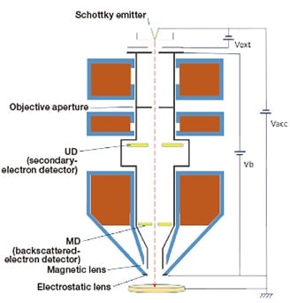
Fig. 1 Schematic diagram of the SU7000 optics system
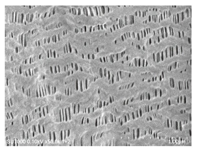
Fig. 2 Example image of separator
Accelerating voltage: 100 V
Magnification: 50,000×
In recent years it has become standard for SEM instruments to be equipped with multiple detectors for secondary electrons and backscattered electrons. This has the advantage of allowing the acquisition of valuable information based on the properties of the detector selected, but requires that the optimal WD and other conditions be separate for each detector. This makes it difficult to achieve high throughput data acquisition.
To ensure high throughput, the optics and detection systems of the SU7000 are specifically designed to allow signal acquisition of all detectors at a single WD (=6 mm). Figure 3 shows the detector layout.
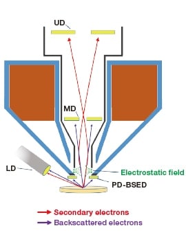
Fig. 3 Schematic diagram of the SU7000 detector system
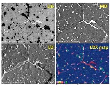
Fig. 4 Specimen observation of an aluminum alloy with signals from all three detectors plus EDX mapping data acquired under identical conditions
Parts of the secondary-electron and backscattered-electron signals emitted from the specimen follow energy-dependent trajectories determined by the electrostatic and magnetic fields of the objective lens; these are detected by UD and MD respectively.
Also, electrons emitted at angles that avoid capture by the objective lens are detected by the LD or PD-BSED. The ability to capture all of these signals with a single WD allows more rapid acquisition of information from the specimen. Moreover, the design of the instrument allows EDX analysis data to be acquired with the 6 mm WD as well. Thus, all aspects of the measurement process—from the choice of specimen regions to observe, to the analysis of material
composition—are accelerated.
Figure 4 shows an example image of an aluminum alloy subjected to thermal treatment after polishing. In this observation, the UD, MD, and LD detector images and the EDX map were all acquired at WD = 6 mm.
From the MD (backscattered-electron) image (upper right) we see that the precipitate is distributed at grain boundaries and within grains. The UD (low-energy secondary-electron) image (upper left) reveals dark regions, not visible in the MD image, that are distinguishable as regions of different contrast. The LD (high-energy secondary-electron and backscattered-electron) image (lower left) gives topographical information of same regions.
Because we are able to acquire EDX mapping data (lower right) without changing any acquisition conditions, we confirm that the dark regions are oxides of magnesium and silicon (yellow-green parts). Because magnesium and silicon oxides are relatively close in average atomic number to the aluminum (matrix), they do not exhibit high contrast in the MD image. On the other hand, UD is sensitive to low-energy secondary electrons, and we conclude that difference in secondary-electron emission efficiency between metals and oxides results in high contrast.
As seen above, simultaneous signal acquisition with various detectors enables rapid accumulation of multifaceted information.
For the purpose of understanding the behavior of materials under processing, techniques for making dynamic observations—such as in-situ observations—have long been in high demand. For information on material composition and crystallographic structure, high-speed acquisition of the backscattered-electron signal is required. The SU7000's newly developed semiconductor detector for backscattered electrons—the PD-BSED—features improved responsiveness and higher image quality for dynamic observations at high scan rates.
Figure 5 shows a case-study observation of foreign particles on a silicon substrate, observed with the PD-BSED.
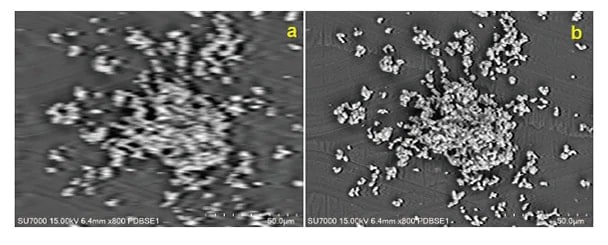
Fig. 5 Comparison of responsiveness for backscattered electron detector, the PD-BSED
In the conventional observation (a), due to streaking in the image, the shape of the particles is not discernible. Using the new PD-BSED detector (b), the shape of the particles is clearly observable.
In addition to the rapid responsiveness of the new detector, the SU-7000 is also equipped with a specimen chamber and a stage capable of mounting heavy items such as tensile stage, further expanding the range of options for in-situ and other types of dynamic behavior observations.
The specimen chamber of the SU7000 offers a total of 18 accessory ports to allow a variety of optional accessories.
The SU7000 delivers the following features:
In addition to the acquisition of conventional static SEM images and microanalysis, the design and functionality of the SU7000—engineered with an eye toward dynamic observations—will help users expand and redefine the boundaries of what is possible in SEM.
About the author
Shigeaki Tachibana
Metrology and Analysis System Division
Nano-Technology Solution Business Group
Hitachi High-Tech Corporation
See more
