Yutaka Nagaoka*1, Tatsuya Hirato*2
A scanning electron microscope (SEM) is an instrument that detects the signal generated while scanning an electron beam across a specimen surface to image. The signals that can be obtained by electron beam irradiation include secondary electrons (SEs), backscattered electrons (BSEs), characteristic X-rays, and cathodoluminescence (CL), and since these make it possible to perform a detailed surface analysis of the sample, the SEM is used in a variety of fields from semiconductor device analysis to materials development.
However, when a nonconductive specimen is observed, the specimen surface becomes charged by the incident electrons, and imaging artifacts such as abnormal contrast and image drift occur. Low-vacuum SEM observation has been developed as a method to avoid or to mitigate these problems. In the low-vacuum SEM, positive charges generated by collisions between incident electrons and residual gas molecules inside the chamber act to neutralize the negative charge on the specimen surface, reducing the effect of charging. Since it is difficult to detect low-energy SEs by observation in the low-vacuum range, Hitachi has developed an ultra variable-pressure detector (UVD) for the low-vacuum SEM, which can detect SEs under low-vacuum conditions1) . In addition to the SE detector functionality,
applications that utilize the features of this UVD were also developed. This paper describes examples of using the UVD for CL observations of materials and for scanning transmission electron microscope (STEM) observations of nanomaterials and liquid specimens.
Figure 1(a) shows a schematic diagram of the UVD. In order to efficiently detect SEs generated from the specimen when it is irradiated by an electron beam under a low vacuum, a bias voltage is applied to the detector front edge. This forms an electric field between the detector and the specimen, which accelerates the SEs generated at the specimen surface. The SEs then collide with the residual gas molecules in the low-vacuum environment, ionizing the molecules into positive ions and electrons while simultaneously generating light. By detecting this light using the UVD during the beam scanning, images that reflect topological information about the specimen surface can be captured.
Figure 1(b) shows the results of observation of a fracture surface of carbon fiber reinforced plastic (CFRP) using a UVD mounted on a model SU3800 tungsten SEM (W-SEM) system. The detailed surface roughness of the resin fracture surface and the state of the resin around the carbon fibers could be observed in the low-vacuum condition while suppressing charging. In order to respond to a wide range of needs, Hitachi have been able to provide the UVD in a range of microscopes from a W-SEM system equipped with a thermal electron gun to a field emission SEM (FE-SEM) system equipped with a Schottky electron gun.
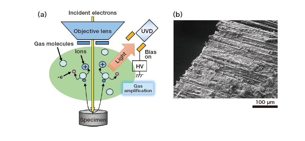
Fig. 1 (a) Schematic diagram of UVD signal detection. (b) UVD image of CFRP
Since information such as the crystallinity and chemical properties of a specimen can be obtained by measuring CL, which is generated by irradiating the specimen with an electron beam, it is used for analysis of specimens such as semiconductors, ceramics, minerals, and fluorescent materials. The UVD is also capable of detecting CL information. CL images can be captured using the UVD by turning off the bias voltage applied to the detector front edge. As a result, the light that carries the secondary electron information as described in the previous section can no longer be detected, and only the CL signal generated from the specimen is detected. Figure 2 shows an example of observing crystal dislocations (defects) in gallium nitride (GaN) which is used in power emiconductors with a model SU5000 FE-SEM. When a GaN substrate is irradiated by an electron beam, areas of good crystallinity generate CL and appear bright, while areas containing threading dislocations do not emit light and appear dark. The black dots in Figure 2 correspond to areas where no light has been emitted due to the presence of dislocations, and this shows that dislocations in GaN can be clearly identified.
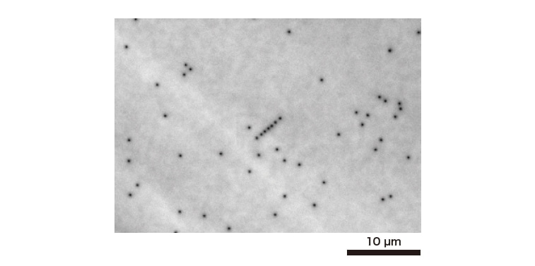
Fig. 2 CL observation results for gallium nitride substrate (accelerating voltage: 5 kV) (Specimen provided by courtesy of Associate Professor Yoshio Honda, Center for Integrated Research of Future Electronics, Institute of Materials and Systems for Sustainability, Nagoya University)
Next, another example of CL observation for titanium dioxide (TiO2) nanoparticles is described. TiO2 nanoparticles exist as a rutile type and an anatase type, and the anatase type is used as a photocatalyst. Since the differences between these are only in the crystal structure, differentiating them by only SEM observation is difficult. However, the CL emission intensity for anatase is higher than that for rutile, and the brighter emission can be distinguished by CL observation using the UVD. Figure 3 shows the results of observing a mixture of rutile and anatase TiO2 nanoparticles using a model SU7000 FE-SEM system. Although no difference can be distinguished in the SE (a) or BSE (b) images, in the CL image (c) it can be seen that some of the particles emit light. Furthermore, the particles that emit light can be identified by overlaying the CL image on the BSE image (d). CL observation using the UVD enables a wide variety of applications such as, observation of crystal defects in semiconductors, observation of the zircon zonal structure in mineral samples, investigation of high purity alumina samples, or evaluation of fluorescent materials.
![Fig. 3 Observation results for titanium dioxide nanoparticles (accelerating voltage: 3 kV) [(a) SE image. (b) BSE image. (c) CL image. (d) Overlay of CL image on BSE image]](/image/global/sinews/technical_explanation/130312/index_03.jpg)
Fig. 3 Observation results for titanium dioxide nanoparticles (accelerating voltage: 3 kV) [(a) SE image. (b) BSE image. (c) CL image. (d) Overlay of CL image on BSE image]
STEM observation by an SEM uses the electron optics of the SEM system as-is, and detects transmission electrons from a thin-film specimen placed on a TEM grid. As general SEMs use an accelerating voltage of 30 kV or less, it is also called low-voltage STEM, and there are considerable electrons scattered even in low-density specimens, which can be observed with high contrast2) . We now introduce a new STEM holder3) that enables bright-field STEM observation using the UVD.
Figure 4 shows a schematic diagram of the new STEM holder. In this holder, a scintillator is placed under the specimen, and a bright-field STEM image is formed by detecting the light generated when electrons transmitted through the thin-film specimen collide with the scintillator by the UVD. This holder can detect only the light generated by transmission electrons more efficiently than existing metal plate reflective STEM holders, thus making it possible to observe STEM images at a high S/N ratio.
Figure 5 shows the results of observing magnetic nanoparticles with a model SU5000 FE-SEM system using this STEM holder and the results of measuring the particle sizes by image analysis software. Although the accelerating voltage is only 30 kV, small particles with sizes of several tens of nanometers were observed clearly. Furthermore, image processing was performed using the image analysis software Image-Pro (Media Cybernetics), and the diameters of the nanoparticles and the particle size distribution were analyzed. By using STEM images, errors associated with overlapping particles could be reduced.
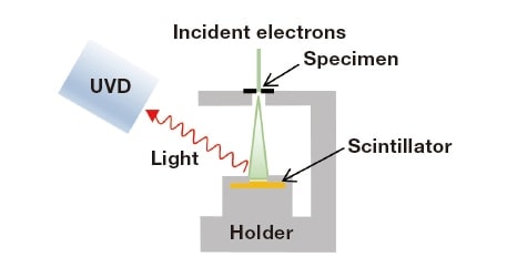
Fig. 4 Schematic diagram of STEM holder
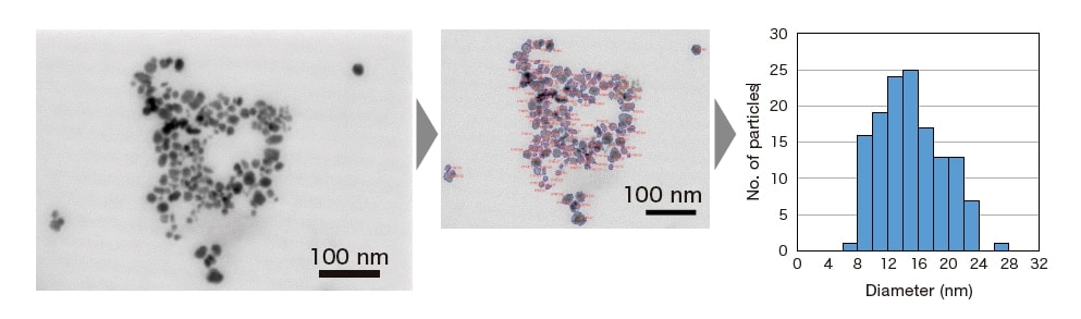
Fig. 5 Observation and particle size distribution results for magnetic nanoparticles using STEM holder (accelerating voltage: 30 kV) (Specimen provided by courtesy of Professor Toru Maekawa, Bio-Nano Electronics Research Center, Toyo University)
Next, we introduce an example of observing a liquid specimen using the STEM holder and liquid observation holder. In this experiment, the K-kit (made by Bio MA-Tek), which has been commercialized as a liquid observation capsule, was used. This is a capsule made of silicon with silicon nitride membranes through which observations are enabled. The liquid specimen is filled from the injection port into the capsule by capillary action and sealed with adhesive to maintain a liquid state in the SEM chamber. The observation region is at the center of the holder. An area in the region is irradiated by the electron beam, and the transmitted electrons are detected.
Figure 6 shows the results of STEM observations of a slurry with a particle size of 40 nm using a model SU3900 W-SEM system. Figure 6(a) shows the results of observation of a dried slurry dripped onto a mesh with a collodion membrane, the slurry particles agglomerated during the drying process, making it difficult to observe the dispersed state. In contrast, Figure 6(b) shows the results of observing a slurry injected and sealed using the K-kit, which shows that well-dispersed slurry particles can be observed as black dots. Thus, the dispersal state of particles in liquid can be clearly observed even by STEM observation using an SEM.
![Fig. 6 Results of STEM observation of a slurry (accelerating voltage: 30 kV) [(a) Dripped onto mesh. (b) Using K-kit]](/image/global/sinews/technical_explanation/130312/index_06.jpg)
Fig. 6 Results of STEM observation of a slurry (accelerating voltage: 30 kV) [(a) Dripped onto mesh. (b) Using K-kit]
This paper introduced examples of observations using the UVD which can be installed in W-SEM and FE-SEM systems. It was shown that positions of threading dislocations in a GaN substrate and the anatase types among TiO2 nanoparticles can be distinguished by CL observations. Using STEM, it was shown that magnetic nanoparticles could be imaged and the particle size distribution could be determined using the newly developed STEM holder, and liquid specimens could be observed using a combination of the K-kit and the STEM holder. The UVD not only functions as a secondary electron detector under low-vacuum conditions, but is a multifunction detector that can also capture CL images and STEM images, which conventionally require specialized detectors. The authors anticipate that SEM systems equipped with the UVD will contribute to the improvements of semiconductor device performance and the developments of novel functional nanomaterials.
References
Publication data
Published in the monthly journal Engineering Materials (December issue 2020)
About the author
Analysis Systems Solution Development Department
Metrology and Analysis Systems Product Division
Nano-Technology Solution Business Group
Hitachi High-Tech Corporation
Control Systems Design Department
Metrology and Analysis Systems Product Division
Nano-Technology Solution Business Group
Hitachi High-Tech Corporation
See more
