Hiroaki Matsumoto, Hiromi Inada
In the development of nanomaterials for energy and environmental applications, a key role is played by environmental transmission-electron microscopy (ETEM). ETEM allows variations in the fine-grained structure of specimens to be observed in real time, in situ, and with high spatial resolution, under environments closely resembling the operating environments of actual catalytic materials—making it a powerful tool for identifying the causes of material degradation, for determining reaction mechanisms, and for analyzing other key phenomena1-4). In particular, recent years have witnessed intense interest in, and growing demand for, ETEM analysis of electrode catalysts under various gaseous atmospheres and high-temperature environments, for purposes such as enhancing the power-generation performance and durability of hydrogen cells and other fuel cells and improving the electrolysis performance of solid-oxide electrolysis cells (SOECs). In this article we focus on one particular choice of electrode catalyst for SOEC cathodes: perovskite oxides, which are known to exhibit high activity and good stability.
SOECs—high-temperature electrolytic systems that can use wind, solar, or other renewable energy sources to convert carbon dioxide (CO2) into reusable forms of energy such as carbon monoxide (CO) or hydrogen (H2)— offer great promise for CO2 capture, energy recycling, and other techniques for promoting carbon neutrality5). To improve CO2 electrolysis performance, a catalyst structure has been proposed in which copious quantities of metallic nanoparticles are dispersed over the perovskite surface; for such structures, understanding the mechanism through which metal nanoparticles form on the perovskite catalyst surface in the presence of redox reactions is an important prerequisite for increasing catalytic activity and controlling stability6). For this purpose, in this study we develop a technique for in-situ observation of specimen surfaces on sub-nanometer length scales via aberration-corrected secondary electron (SE) imaging with atomic resolution; we demonstrate the use of this technique by acquiring simultaneous high-resolution in-situ scanning TEM (STEM) and SE images of specimen surfaces and the internal specimen structure under gaseous atmospheres.
In this article, we first describe our measurement system—the Hitachi High-Tech HF5000 transmission electron microscope, featuring an automated aberration corrector and capable of high-resolution STEM/SEM observation at an accelerating voltage of 200 kV, and equipped with a microelectromechanical systems (MEMS)-based heated specimen holder —and then use this system to investigate an SOEC electrode catalyst. Because our technique uses STEM and SEM for environmental STEM observations, we refer to it as ESTEM.
This article is a revised version of content published in Nature Communications with our collaborators Professor Guoxiong Wang and Dr. Houfu Lv of the Dalian Institute of Chemical Physics (Lv, H. et al., Nature Communications, 12, 5665 (2021)); some figures from that publication are also reproduced here.
We also note that other studies of SOEC perovskite electrode catalysts using the apparatus described in this article have been published elsewhere7,8).
For this study we used the HF5000 TEM/STEM system from Hitachi High-Tech (Figure 1) 9). Designed for elemental analysis and image acquisition at nanometer and atomic length scales for research and development related to highly functional materials and other fields, the HF5000 features a cold-cathode field-emission electron gun and a probeforming automated aberration corrector achieving an STEM resolution of 78 pm (at an accelerating voltage of 200 kV). The aberration corrector corrects the spherical aberration of the electron lens, focusing the electron beam that irradiates the specimen surface to atomic-scale probe sizes; the high probe current enables high-resolution STEM observation and high-sensitivity elemental analysis mapping via energy dispersive X-ray spectroscopy (EDX) and other techniques. In addition to its TEM observation capabilities, the HF5000 is equipped with annular-dark-field (ADF), bright-field (BF), and secondary electron (SE) detectors and can capture images from all three of these signals simultaneously, providing information on atomic-number-dependent contrast, surface morphology, and the internal structure of specimens. The ability to capture SE images with atomic resolution—a key advantage of the HF500010-12)—yields atomic-scale surface information and three-dimensional information on catalyst nanoparticles and their supports. For two-dimensional EDX mapping of elemental distributions, the system features two windowless silicon-drift X-ray detectors (Oxford Instruments X-Max 100LE, effective detector area 100 mm2), minimizing the dependence on specimen orientation to achieve high detection sensitivity even for light elements. For analysis of chemical states, the system also includes an electron energy-loss spectroscopy (EELS) analyzer (Gatan Quantum ER 965).
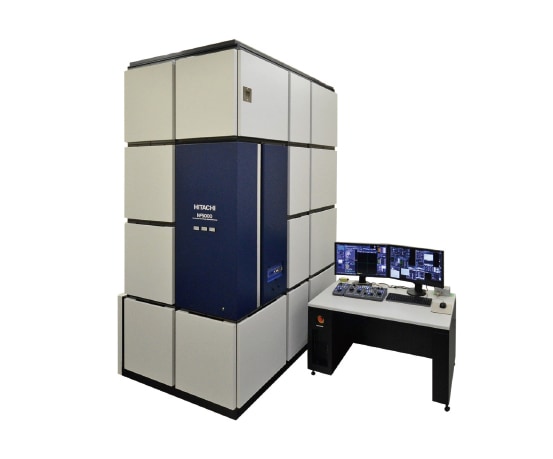
Fig. 1 The HF5000 200 kV FE-TEM/STEM/SEM system from Hitachi High-Tech.
There are two approaches to environmental TEM: the diaphragm method, which uses thin films of carbon or silicon nitride as windowing materials to trap gases in the vicinity of the specimen, and the selective-exhaust method, in which gases are directly injected through orifices into the specimen chamber and vacuum pumps are used to remove gas that has leaked into other sectors of the instrument, thus simultaneously achieving a gaseous atmosphere in the specimen chamber while maintaining a high vacuum for the electron gun.
Each of these approaches requires various custom modifications to the apparatus, including orifices, diaphragms for mirror units, and vacuum-exhaust systems1-4). In the diaphragm approach, diaphragms are placed above and below the specimen mount of a side-entry specimen holder; this has the advantage of allowing the introduction of gaseous atmospheres relatively easily and without major modifications to the TEM system, but the passage of the electron beam through diaphragms creates scattering effects that may degrade image quality.
The selective-exhaust approach places restrictions on the quantity of gas that may be introduced—and is thus limited to lower gaseous-atmosphere pressures than can be achieved by diaphragm techniques—but minimizes the impact of electron-beam obstruction due to the diaphragm. This consideration is of particular importance for ETEM, which requires both elemental analysis and secondary electron imaging of surfaces.
For our apparatus we adopt the selective-exhaust approach. In addition, to enable atomic-scale analysis of environmental STEM results, we improve the vacuum-exhaust system of the aberration-corrected TEM/STEM instrument to allow direct injection of gas into the mirror unit (Figure 2). We do this by adding a gas-injection nozzle to the specimen chamber, positioned to ensure that the distance from the nozzle tip to the specimen is less than 5 mm; this allows gas to be sprayed directly into the vicinity of the specimen. The injected gas and reaction gases are continuously removed by a turbomolecular pump, maintaining an atmosphere of fresh reaction gas (at a pressure of around 10 Pa) surrounding the specimen. The orifices used for the selective-exhaust system are positioned at locations that do not interfere with observation or analysis. Gas-injection conditions are easily configured through a GUI control system. In designing this apparatus, we took pains to ensure that our measurement system was not limited to the special case of environmental observations, but rather retained the full observational and analytical performance of standard electronmicroscope systems. Our ESTEM approach is based on STEM—with the electron beam tightly focused to yield a narrow probe—to enable surface observation and analysis at nanometer and atomic length scales.
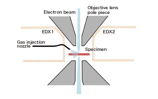
Fig. 2 Schematic diagram of TEM specimen chamber indicating the relative positioning of the specimen, the two EDX detectors, and the gas-injection nozzle.
Figure 3 shows the MEMS-based heated specimen holder used in this study, which exploits semiconductor MEMS technology to achieve heating temperatures as high as 1,100°C over a heated region approximately 20 μm in size13,14). The extremely small size of the heated region ensures that heating-induced specimen drift is sufficiently well-stabilized to allow nanoparticle observation and analysis. The MEMS heating chip may be removed and reinserted, facilitating instrument operation. PC-based temperature-control software allows the temperature and its rate of increase or decrease to be configured arbitrarily. One of two heating chips—one with holes in a silicon-nitride film, and the other without holes—may be selected as appropriate for the analysis in question.
Figure 4 outlines the workflow for in-situ observations of heated specimens under gaseous atmospheres using this apparatus. After mounting a MEMS heating chip at the edge of the specimen holder, a powder catalyst specimen is dispersed over the MEMS chip via the ethanol-dispersion method. The specimen holder is then inserted into the specimen chamber and an observation field of view is identified. Once the field of view has been established, images of the initial (pre-reaction) state of the specimen are acquired, after which gas injection is initiated by using the flowcontrol portion of the TEM system user interface to open the gas-injection valve, commencing the spray of gas into the vicinity of the specimen. The gas pressure is indicated in numerical form by a display on the vacuum gauge mounted in the mirror unit. The pressure in the vicinity of the specimen is measured by a pre-installed micro-pressure gauge to monitor correlations between the pressure in the mirror unit and the pressure near the specimen. With this apparatus, reaction processes occurring under gaseous atmospheres and at elevated specimen temperatures may be observed via STEM and SEM images and analyzed via EDX and EELS.
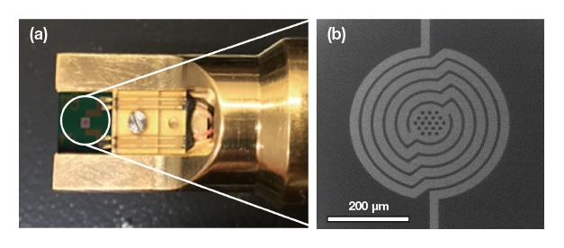
Fig. 3 MEMS-based heated specimen holder for atomic-scale observations. (a) Specimen mount. (b) SEM image of MEMS-based specimen heating unit.
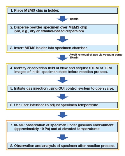
Fig. 4 Workflow for in-situ environmental observations.
We used Sr2Fe1.4Ru0.5Mo0.5O6-σ (SFRuM) perovskite oxide as our experimental specimen. Before SFRuM perovskites can be used to catalyze CO2 electrolysis in SOEC fuel electrodes, they must be subjected to a reduction/oxidation treatment to induce formation of nanoparticles on the crystal surface5,6).
As reported by Lv et al.,6) CO2 electrolysis studies (800°C, 1.2 V) showed that performance improves after the first reduction step and continues to improve through three subsequent repetitions of an oxidation/reduction cycle. SEM observations of powder specimens after each repetition show that during the first reduction step, a large number of nanoparticles form on the surface; during an ensuing oxidation step, these particles disappear, but during another reduction step an even greater number of particles form on the surface. This indicates that the observed improvement in CO2 electrolysis performance is associated with an increasing number of nanoparticles deposited on the perovskite surface.
To investigate the mechanism for nanoparticle formation on the perovskite catalyst surface, we introduced hydrogen and oxygen gases into the specimen chamber of our electron microscope and performed in-situ ESTEM/SEM observations at an accelerating voltage of 200 kV and a probe current of 100 pA, with the pressure in the vicinity of the specimen maintained at up to 10 Pa and the specimen heated to temperatures between 200 and 850°C. In addition, assuming CO2 electrolysis, we also performed in-situ observations under a CO2 gas atmosphere. The results of these observations are discussed in the following sections.
Figure 5 shows SE images, ADF-STEM images, and STEM-EDX element maps of an SFRuM (O1) specimen [powder specimen after one reduction step (R1) and one oxidation step (O1)] at 800-850°C under a hydrogen gas atmosphere.
At 800°C, between 10 and 60 min after the introduction of hydrogen gas, Ru nanoparticles with an approximate size of 3 nm form on the perovskite surface and along its edge. SE images clearly indicate that the crystalline perovskite surface transforms into a 1-2 nm layered structure [Figure 5(b-d)]. After 15 minutes at 850°C, EDX maps indicate segregation of Fe by approximately 0.5 nm at the Ru particle surface. This suggests an intermediate state in which Fecovered Ru particles disperse stably over the perovskite surface, as shown clearly in the SE image [Figure 5(e)]. As the reaction proceeds, Ru particles transform into RuFe alloy after 800°C/60 min + 850°C/30 min of the reduction process, as indicated by EDX maps and in-situ STEM-EELS analysis (Figure 6).
![Fig. 5 In-situ observations of SFRuM (O1) specimen (800-850°C, hydrogen gas atmosphere). (a) 800°C, 10 min. (b) 800°C, 60 min. (c) 800°C, 15 min. (d) 800°C, 15 min. (e) 850°C, 15 min. [From Lv, H. et al ., Nature Communications, 12, 5665 (2021) with modifications.]](/image/global/sinews/technical_explanation/130317/index_05.jpg)
Fig. 5 In-situ observations of SFRuM (O1) specimen (800-850°C, hydrogen gas atmosphere). (a) 800°C, 10 min. (b) 800°C, 60 min. (c) 800°C, 15 min. (d) 800°C, 15 min. (e) 850°C, 15 min.
[From Lv, H. et al ., Nature Communications, 12, 5665 (2021) with modifications.]
![Fig. 6 In-situ observations of SFRuM (O1) specimen under hydrogen gas atmosphere at 800°C after 60 min and 850°C after 30 min. (a) ADF-STEM image. (b) EDX elemental map. (c) STEM-EELS analysis. [From Lv, H. et al ., Nature Communications, 12, 5665 (2021) with modifications.]](/image/global/sinews/technical_explanation/130317/index_06.jpg)
Fig. 6 In-situ observations of SFRuM (O1) specimen under hydrogen gas atmosphere at 800°C after 60 min and 850°C after 30 min. (a) ADF-STEM image. (b) EDX elemental map. (c) STEM-EELS analysis.
[From Lv, H. et al ., Nature Communications, 12, 5665 (2021) with modifications.]
Figure 7 shows in-situ STEM/SEM images and EDX element maps of the RuFe alloy particles discussed in the previous section, at 200°C under an oxygen gas atmosphere. We focus on the particle indicated in Figure 7(a,b). At 70 s after the introduction of oxygen gas, we observe the formation of an Fe oxide film over the RuFe particle surface [Figure 7(c,e)].
At 800°C, after 30 min under an oxygen gas atmosphere, the SE image shows an ordered pattern of facets on the Ru particle [Figure 8(b)], while BF-STEM and ADF-STEM images indicate that the Ru particle exhibits extensive crystallinity [Figure 8(c,d)]. After 60 min at 800°C under an oxygen gas atmosphere, the Ru particle has fully dissolved into the perovskite interior.
![Fig. 7 In-situ observations of RuFe alloy nanoparticle under oxygen gas atmosphere (200°C, after 70 s). (a) SEM image. (b) ADF-STEM image. (c,d,e) STEM-EDX maps. [From Lv, H. et al ., Nature Communications, 12, 5665 (2021) with modifications.]](/image/global/sinews/technical_explanation/130317/index_07.jpg)
Fig. 7 In-situ observations of RuFe alloy nanoparticle under oxygen gas atmosphere (200°C, after 70 s). (a) SEM image. (b) ADF-STEM image. (c,d,e) STEM-EDX maps.
[From Lv, H. et al ., Nature Communications, 12, 5665 (2021) with modifications.]
![Fig. 8 In-situ observations of Ru nanoparticle under oxygen gas atmosphere (800°C, after 30 min). (a,b) SEM images. (c) BF-STEM image. (d) ADF-STEM image. [From Lv, H. et al., Nature Communications, 12, 5665 (2021) with modifications.]](/image/global/sinews/technical_explanation/130317/index_08.jpg)
Fig. 8 In-situ observations of Ru nanoparticle under oxygen gas atmosphere (800°C, after 30 min). (a,b) SEM images. (c) BF-STEM image. (d) ADF-STEM image.
[From Lv, H. et al., Nature Communications, 12, 5665 (2021) with modifications.]
Figure 9 shows STEM/SEM images and EDX maps of an RuFe alloy particle (formed at 850°C under a hydrogen gas atmosphere) at 200°C after 30 min under a CO2 gas atmosphere. A low-contrast region of amorphous material can be seen at the RuFe/SFRuM interface, indicating the occurrence of CO2 gas adhesion reactions at that interface.
![Fig. 9 In-situ observations of RuFe alloy nanoparticle under CO2 gas atmosphere (10 Pa) (200°C, 30 min). (a) BF-STEM image. (b) SEM image. (c) Overlay of C and Ru EDX maps. (d) EDX maps. [From Lv, H. et al., Nature Communications, 12, 5665 (2021) with modifications.]](/image/global/sinews/technical_explanation/130317/index_09.jpg)
Fig. 9 In-situ observations of RuFe alloy nanoparticle under CO2 gas atmosphere (10 Pa) (200°C, 30 min). (a) BF-STEM image. (b) SEM image. (c) Overlay of C and Ru EDX maps. (d) EDX maps.
[From Lv, H. et al., Nature Communications, 12, 5665 (2021) with modifications.]
In this article we presented a technique for atomic-scale in-situ observation of changes in the surface and in the internal structure of SOEC perovskite catalysts using the HF5000 gaseous-atmosphere-controlled aberration-corrected 200 kV STEM/SEM system with a MEMS-based heated specimen holder. Using this technique, we performed in-situ observations to elucidate the mechanisms responsible for promoting the deposition of RuFe particles under reducing atmospheres. We showed that, under a reducing atmosphere, Ru atoms in SFRuM preferentially migrate to the perovskite surface and form Ru nanoparticles, after which a reaction process occurs in which Fe atoms migrate to the surfaces of Ru particles to form intermetallic RuFe compounds. Subsequently, under an oxidizing atmosphere, Fe atoms in the RuFe alloy preferentially oxidize and return to the perovskite, after which Ru atoms migrate to the SFRuM surface. Repeated application of these oxidation and reduction steps has the effect of enriching the Ru concentration beneath the SFRuM perovskite surface. We expect our in-situ ESTEM/SEM observation technique to be useful for characterizing not only perovskite electrode catalysts, but also for various other types of functional nanomaterials and catalysts. It may be combined with electrochemical characterization techniques to yield rapid feedback during the material-development process.
Acknowledgements
We are grateful to Professor Guoxiong Wang and Dr. Houfu Lv of the Dalian Institute of Chemical Physics for providing the specimens used in this study and for valuable discussions regarding the results of collaborative experiments.
References
Publication data
Reprinted from Nenryo Denchi Vol. 21 No. 3 (2022) p.14–19 (in Japanese)
About the authors
Hiroaki Matsumoto, Hiromi Inada
Beam Technology & Analytical Systems Product Division
Core Technology & Solutions Business Group
Hitachi High-Tech Corporation
