Yuki Inagi
Ion milling is a technique for preparing cross-sectional sample for observation via scanning-electron microscopy(SEM). The ease with which this approach can produce cross-sectional surface—without applying stress to the sample—has made it a widely-used tool in many fields of science and engineering, from semiconductor research to electronics and material science. In recent years, the increasing complexity of the sample structures observed by SEM, together with growing demand for streamlined workflows and improved operational efficiency, have created a need for sample-preparation techniques capable of handling a diverse variety of samples—while reducing the time required to prepare samples for observation.
Two varieties of ion milling are commonly used to prepare SEM samples: cross-section ion milling and flat ion milling.1) Hitachi High-Tech offers two hybrid ion-milling systems—the ArBlade5000 and the IM4000II, shown in Figure 1—with both systems supporting both types of milling. In this article, we first survey the basic principles of ion milling, then discuss the capabilities of Hitachi's newest ion-milling systems and present a number of illustrative applications.
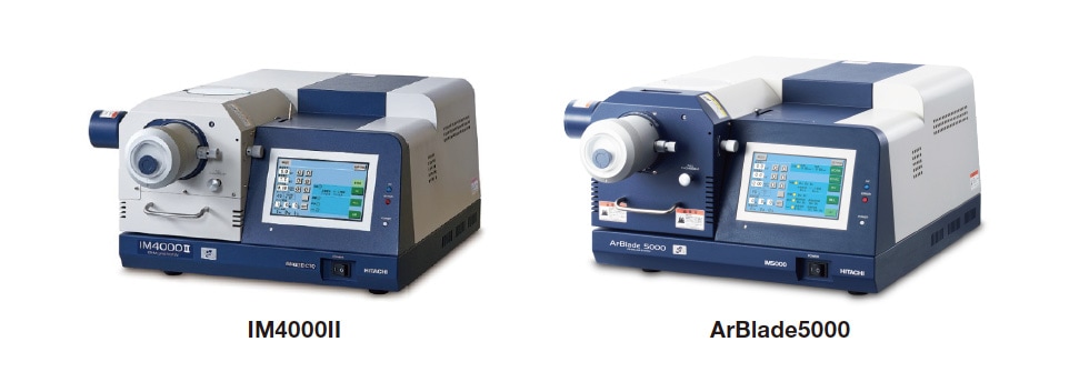
Fig. 1 IM4000II (left) and ArBlade5000 (right) ion-milling systems.
Ion milling exploits the phenomenon of sputtering—in which a sample is irradiated by a broad, unfocused ion beam from an ion gun, causing atoms to be ejected from the sample surface—to yield observation surfaces that are smooth over length scales on the order of millimeters.2) In general, argon gas, which induces minimal chemical transformation for most samples, is used as the ion source.
In cross-section milling, as shown in Figure 2, the ion beam is partially obstructed by a beam-blocking slab (known as a mask) placed between the ion gun and the sample, so that only the portion of the sample extending beyond the mask is irradiated. In this case, sputtering proceeds along the edge of the mask, removing the exposed portion of the sample and leaving behind a smooth cross-sectional surface. Typically, the sample is positioned with 10-100 μm of its length extending beyond the mask, and the sample holder is rotated over a swing angle of ±15-40° to avoid inducing line defects.
In general, cross-section milling is an effective tool for preparing observation-ready cross sections of samples that are difficult to polish mechanically, including hybrid samples comprising multiple distinct materials or fragile samples
incorporating large numbers of voids.
The effectiveness of cross-section milling is illustrated by Figure 3, which shows cross-sectional surfaces of a thermal-paper sample prepared for SEM observation by (a) cutting with a razor blade and (b) cross-section milling. The structure of thermal-paper consists of multiple material layers—including heat-sensitive layers and protective layers—stacked atop a base paper material; in Figure 3(a) it can be seen that the stress exerted on the sample by razor blade cutting has collapsed the various material layers, preventing accurate SEM observation of the layer structure. In contrast, Figure 3(b) shows that the ability of cross-section milling to prepare cross-sectional surfaces without subjecting samples to stress has preserved the layer structure of the thermal-paper, allowing precise observation of layer thicknesses and the dispersion of filler material.
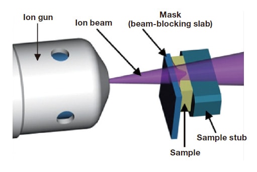
Fig. 2 Schematic depiction of cross-section milling.
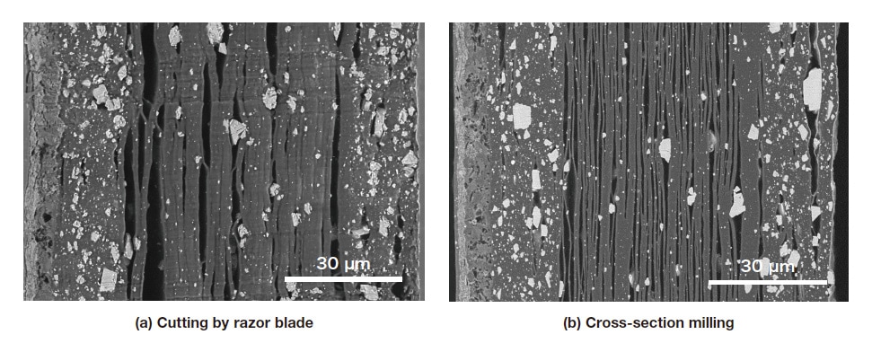
Fig. 3 Cross-sectional SEM images of thermal-paper.
In flat ion milling (or simply flat milling), illustrated in Figure 4, a broad ion beam is trained on a sample surface at a given angle of incidence, allowing large areas of samples to be processed simultaneously. The incidence angle θ may be set anywhere between 0 and 90 degrees; for incidence angles above 80°, the ion beam is nearly parallel to the sample surface, yielding a smooth processed surface and minimizing surface roughness due to variations in etching rate for regions of differing crystal orientation or material composition. This approach is used to eliminate abrasion defects induced by machine polishing of resin-embedded samples. On the other hand, selecting low incidence angles below 45° has the effect of accentuating surface protrusions and indentations due to differences in etching rate; this is useful for purposes such as characterizing the distribution of particles or material grains throughout a sample.
Figure 5 shows SEM images of (a) a mechanically-polished surface of a copper plate, and (b) a surface of the same plate that was subjected to flat milling after mechanical polishing. For the sample prepared by mechanical polishing alone, it can be seen in Figure 5(a) that crystal grains are difficult to observe due to residual polishing defects and strain effects. In contrast, Figure 5(b) shows that the flat milling step eliminates polishing defects and stress-induced distortion layers, allowing clear observation of crystal grains.
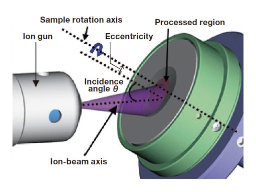
Fig. 4 Schematic depiction of flat milling.
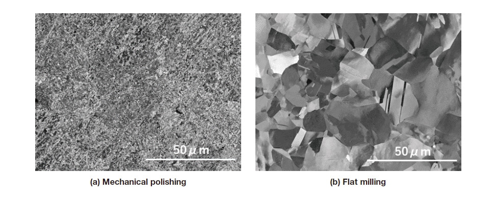
Fig. 5 Cross-sectional SEM images of copper-plate.
The ion-milling systems offered by Hitachi High-Tech are hybrid systems supporting both cross-section milling and flat milling, making them useful for a broad spectrum of applications involving a wide variety of materials. These systems are easily controlled through simple touch-panel interfaces. The range of samples that can be processed by these systems can be further extended by the addition of various optional capabilities, including a cooling mechanism—in which polymeric materials and other samples with low melting points are cooled during the ion-milling process to avoid thermal damage from ion-beam irradiation—and an air protection mechanism for analyzing samples such as lithium-ion battery materials without exposure to the ambient environment.
To illustrate the usefulness of sample cooling, Figure 6 shows the results of cross-sectional processing of a low-melting-point solder sample (a) without cooling (i.e., at room temperature) and (b) with cooling.3) The sample is cooled indirectly using liquid nitrogen and may be maintained at an arbitrary user-specified temperature in the range 0 to −100°C. For the sample processed without cooling, heating due to ion-beam irradiation results in melting of Pb—a metal with a low melting point—yielding the void regions visible in Figure 6(a). In contrast, sample cooling during the milling process restricts the increase in sample temperature, yielding the smooth, defect-free cross-sectional surface shown in Figure 6(b).
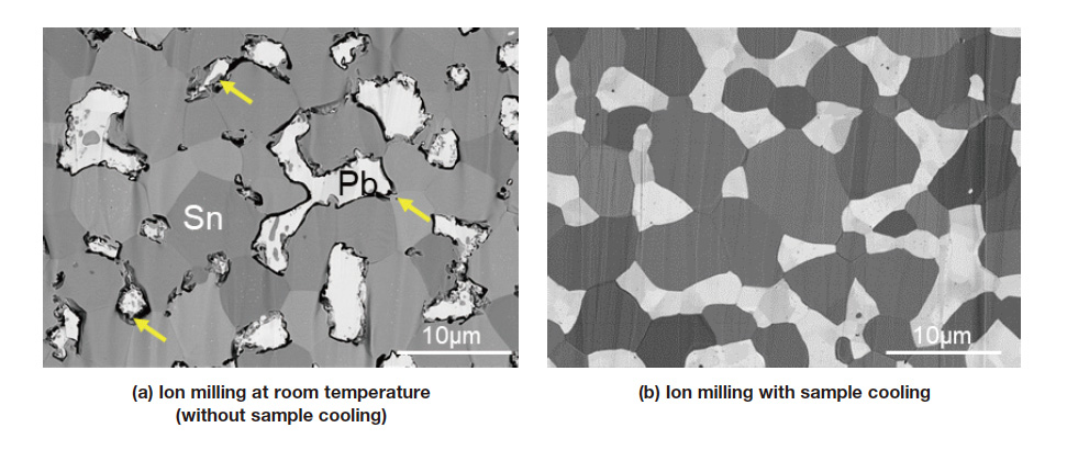
Fig. 6 Cross-sectional SEM images of low-melting-point solder.
For processing samples such as battery materials—which, when exposed to ambient environments, suffer significant shape distortion due to reactions with the oxygen and water present in air—it is convenient to perform ion milling using a hermetically-sealable air protection sample holder. This allows processed cross-sectional surfaces to be analyzed via SEM or atomic-force microscopy (AFM) without exposing samples to the ambient environment. To illustrate the usefulness of this capability, Figure 7(a) shows a SEM image of a lithium-ion battery anode material processed by crosssection ion milling and then transported to the SEM using the air protection mechanism, while Figure 7(b) shows a SEM image of the same sample after environmental exposure.4) For the air protection sample, Figure 7(a) clearly shows the distribution of conduction-assisting agents surrounding graphite. In contrast, in Figure 7(b) it can be seen that, after exposure to the ambient environment, the sample surface is covered by deposits resulting from contact with oxygen and water.
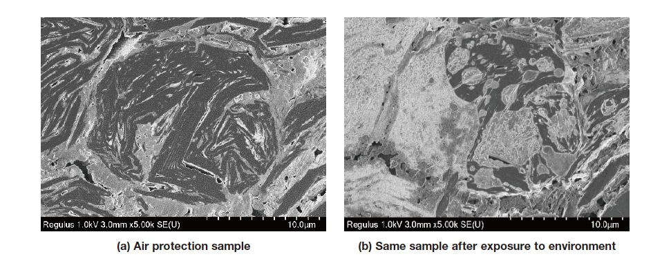
Fig. 7 Cross-sectional SEM images of lithium-ion battery anode.
Conventional cross-section milling systems are capable of processing sample regions with widths of approximately 1 mm. In contrast, the ArBlade5000 boasts wide-area cross-section milling capability that allows preparation of cross sectional surfaces with widths as large as 8 mm. With this capability, a single processing step suffices to prepare smooth cross-sectional surfaces for samples that would require multiple steps with conventional systems, increasing operational efficiency. Figure 8 shows SEM images and energy-dispersive X-ray (EDX) data for a cross-sectional surface of an ultra-hard drill-bit sample processed using the wide-area cross-section milling capability of the ArBlade5000.5) Figures 8(a) and 8(b) respectively show the entire processed surface and an enlarged region of the coating layer, while Figure 8(c) is an EDX map of the enlarged region. The large 8 mm processing range of the ArBlade5000 allowed the entire milling procedure to be completed in 5 hours, demonstrating the ability of this system to prepare large cross-sectional surfaces rapidly via high-throughput processing—even for ultra-hard materials that are difficult to polish. The enlarged image of the surface coating layer reveals a structure consisting of a stack of ultra-thin layers with thicknesses below 50 nm, while the EDX map indicates that this layer stack contains aluminum and titanium. This example demonstrates that wide-area cross-section milling using the ArBlade5000 can yield high-quality cross-sectional surfaces allowing high magnification observation and analysis.
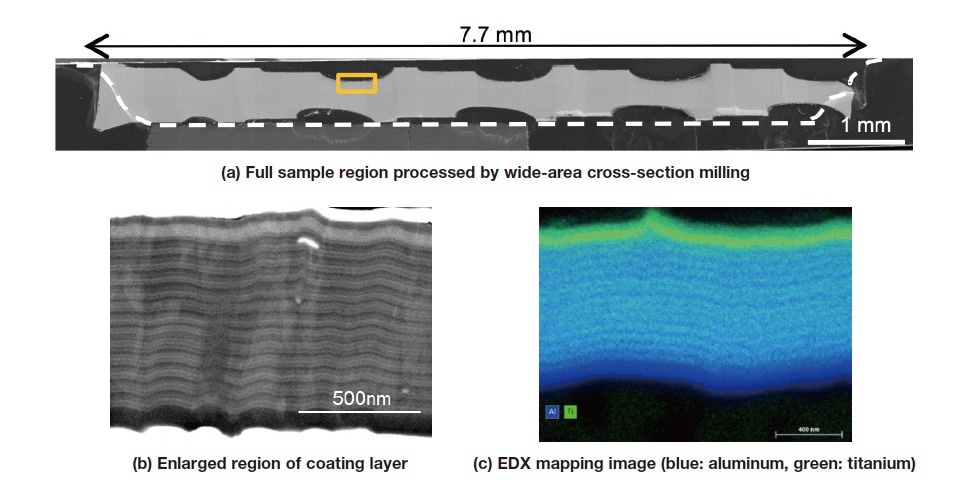
Fig. 8 SEM and EDX images of ultra-hard drill-bit sample prepared for observation by wide-area cross-section milling.
Connecting the ArBlade5000 to a PC allows the system to be controlled by the Advance Control Software (ACS) package, which can transmit and receive processing conditions and compile arbitrary sequences of milling steps to be saved and executed at will. Using the ACS also has the advantage of allowing samples to be processed at multiple sites and under multiple sets of milling conditions. The effectiveness of this capability is demonstrated by Figure 9, an optical microscopy image of an electronic circuit board prepared for observation via ACS multi-site processing. Processing this entire sample via wide-area cross-section milling would be extremely time-consuming, but ACS multi-site processing targets only those sample subregions that require preparation for observation—and processes those subregions under milling conditions optimized for the sample in question—thus preparing cross-sectional surfaces at desired observation sites in just a few hours. Because the system can process samples automatically under arbitrary pre-specified milling conditions, instrument operators are freed from any need to attend to the system until the full processing sequence is complete, reducing processing times and improving operational efficiency.
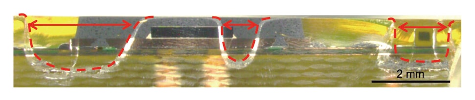
Fig. 9 Optical microscopy image of electronic circuit board sample prepared for observation using multi-site processing capabilities of ACS.
The capabilities of the ACS, when used together with a newly-developed multi-sample holder, allow as many as 3 test samples to be processed in a single milling operation, with milling conditions specified separately for each sample. This reduces the burdensome operations of pumping to achieve a high vacuum and venting to the ambient environment, allowing fully-automated operation of all steps needed to complete the processing of multiple samples—and freeing instrument operators to attend to other tasks while the milling procedure is in progress.
The multi-sample holder, shown in Figure 10, uses spring-loaded sample mounts to hold samples in place via spring action, eliminating any need for hot waxes or pastes.
The usefulness of the multi-sample holder is illustrated by the example in Figure 11, in which the multi-sample holder was used to process three types of test samples: (1) an electronic circuit board, (2) a metal plate with a coating layer, and (3) a thermal-paper sample. Milling conditions were configured separately for each sample; for example, the circuit board and the metal plate were milled for short times at high accelerating voltages, while the thermal-paper was milled at low accelerating voltage to minimize damage due to ion-beam irradiation. Each sample was subjected to a specific sequence of milling steps, including multi-site processing and wide-area cross-sectional processing for the electronic circuit board, for example, both edges were processed, and a region with a width of 3 mm near the left edge was processed via wide-area milling. This example demonstrates the ability of the multi-sample holder to automate complex multi-site milling procedures involving multiple samples, offering significant improvements in operational efficiency.
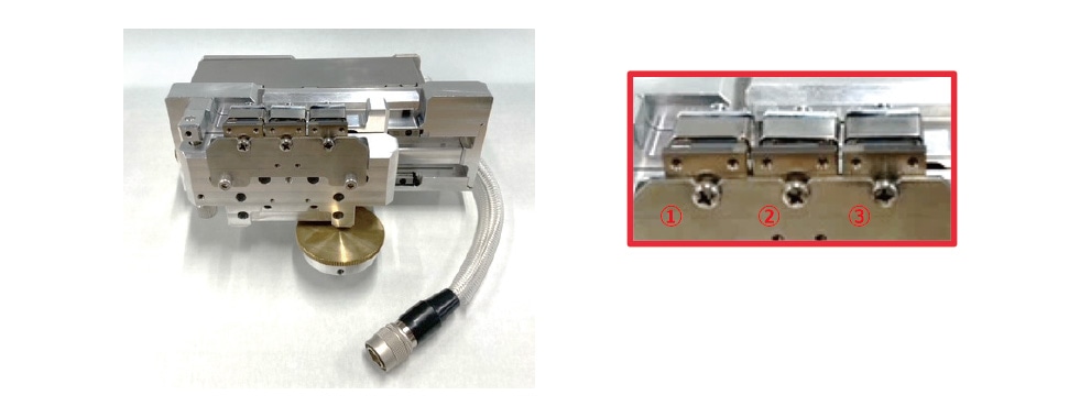
Fig. 10 Multi-sample holder (left) and enlarged view of spring-loaded sample mounts (right).
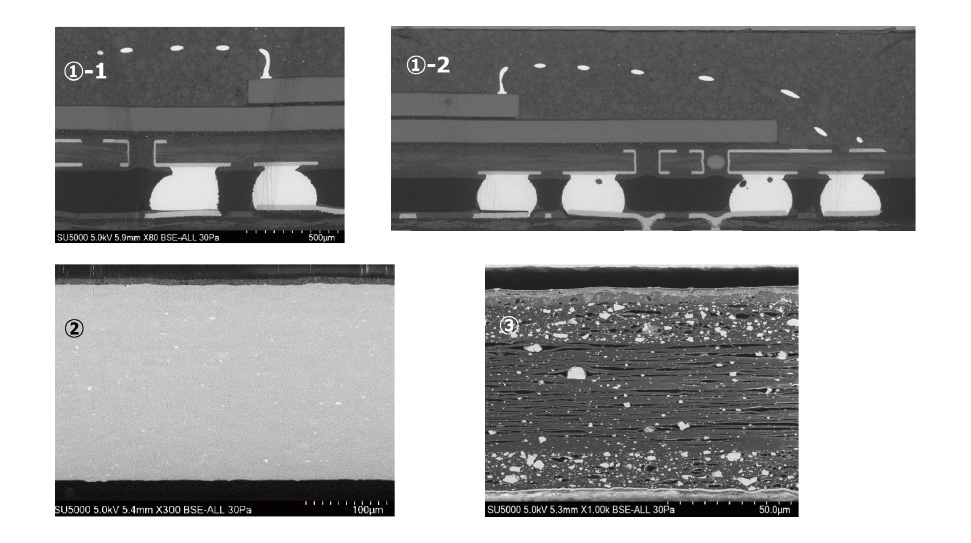
Fig. 11 Multi-sample holder allows one-step processing of multiple test samples: (1) electronic circuit board, (2) metal plate with coating layer, and (3) thermal-paper sample.
Ion-milling systems, augmented by sample-cooling and air protection capabilities, allow preparation of cross sectional observation surfaces for a vast range of samples. The high-throughput operation of Hitachi High-Tech's milling systems reduces the time needed to process samples, while multi-site processing and the multi-sample holder can automate the preparation of cross-sectional surfaces at multiple sites on multiple samples, increasing operational efficiency. These features significantly streamline the preprocessing of SEM observation samples.
References
About the authors
Yuki Inagi
Surface Structure Analysis Group
Solutions Development Department
Beam Technology & Analytical System Products Division
Core Technology & Solutions Business Group
Hitachi High-Tech Corporation
