Takashi Shidara
The rich bounty of information offered by scanning-electron microscopy (SEM), and the relative ease of working with SEM specimens, have made SEM a widely-used tool for measurement, analysis, and observation of fine-grained structure in a broad range of fields, from nanotechnology to semiconductors, electronics, life sciences, and material sciences. Recent advances in information-processing technology have spurred the growth of data-driven R&D models requiring copious input data, creating a demand for SEM techniques capable of quickly and automatically acquiring large quantities of data while reducing the operational burden on users—and the dependence on individual user attributes—required to achieve this automation.
To meet these needs, Hitachi High-Tech developed EM Flow Creator, an automation-support tool capable of flexibly addressing a wide range of requirements across a broad spectrum of fields. In this article we describe key features of EM Flow Creator and illustrate its use through a series of specimen observations.
EM Flow Creator is a software package for creating and executing SEM observation recipes to automate a variety of experimental workflows. Through visual-programming techniques, the tool allows users to implement a variety of programmatic operations—including sequential execution, looping, and conditional branching—via visually intuitive procedures with no coding required.
Figure 1 shows the outline of a typical workflow for an automated observation of multiple specimens, together with a screenshot from an EM Flow Creator session describing this workflow.
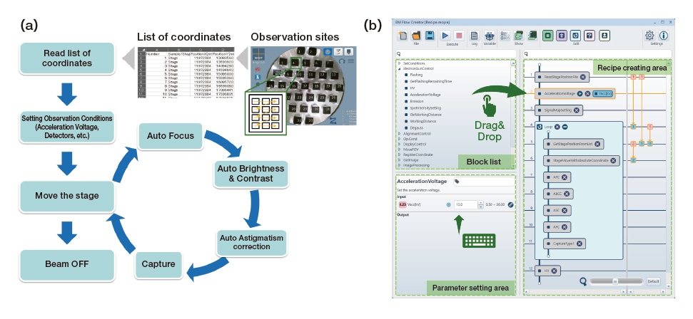
Fig. 1 Typical observation workflow and its description in EM Flow Creator.
(a) Outline of observation workflow. (b) Screenshot of EM Flow Creator session.
To create an SEM observation recipe in EM Flow Creator, users select required procedural blocks from a block list, configure appropriate parameter values for each block, and use a drag-and-drop interface to arrange the blocks in their desired order within a recipe creating area. The block list includes SEM control blocks—such as setting accelerating voltages, translating specimen stages, and autofocusing—together with arithmetic-operation blocks, conditionbased decision blocks, and many other options. Input and output parameters may also be transferred from one block to another [Figure 1(b)]. This allows observation workflows like that in Figure 1(a) to be automated easily without demanding advanced technical skills from users.
Some observation workflows require procedural steps beyond those included in EM Flow Creator’s block list. For such cases, EM Flow Creator can execute scripts written in Python1)—the most popular of the various scripting languages available today—thus allowing extensive customizability.
Figure 2 shows an example of an automated observation of a positive-electrode material for a Lithium-ion Battery(LiB)2). To reduce internal battery resistance, developers of active materials for LiB positive electrodes have reduced particle sizes while increasing packing densities, controlling particle sizes and shapes via SEM particle measurements. In this example, image-recognition techniques were used to search for particles of specific sizes and shapes, with high-magnification surface observations then performed automatically for the selected particles.
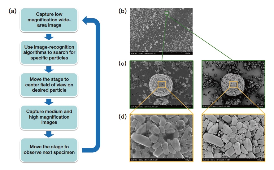
Fig. 2 Automated observation of positive-electrode material for lithium-ion battery.
(a) Outline of observation workflow. (b) 500× secondary electron image. (c) 5k× secondary/backscattered electron image.
(d) 35k× secondary/backscattered electron image.
(Instrument: SU8700. Accelerating voltage: 1 kV. Detectors: Upper and Middle detectors.)
This observation began by acquiring an initial low-magnification (500×) image, then using image recognition to search for a specific particle within the field of view. If a particle closely matching the search criteria was found, the image of the desired particle resulting from the search—indicated by the green rectangle in Figure 2(b)—was saved, after which the specimen stage was translated and the image was shifted to center the field of view on the selected particle, which was then observed simultaneously at intermediate magnification [5,000×, Figure 2(c)] and high magnification [35,000×, Figure 2(d)] via secondary and backscattered electron imaging. The automated procedure encompassed the entire observation: from searching for specific particles, to acquiring an image of the overall particle, to acquiring fine-grained images revealing the structure and composition of the particle surface.
Figure 3 shows an automated multi-specimen observation of LiB separator films at multiple resolutions3,4). Quality-control procedures for LiB production processes require characterization of the thickness, pore structure, and fine-grained surface structure of LiB separators; in this example, multiple specimens fabricated under various manufacturing conditions were simultaneously mounted in an SEM instrument, and images of the specimens were acquired at different magnifications to allow automated comparison of specimen structures.
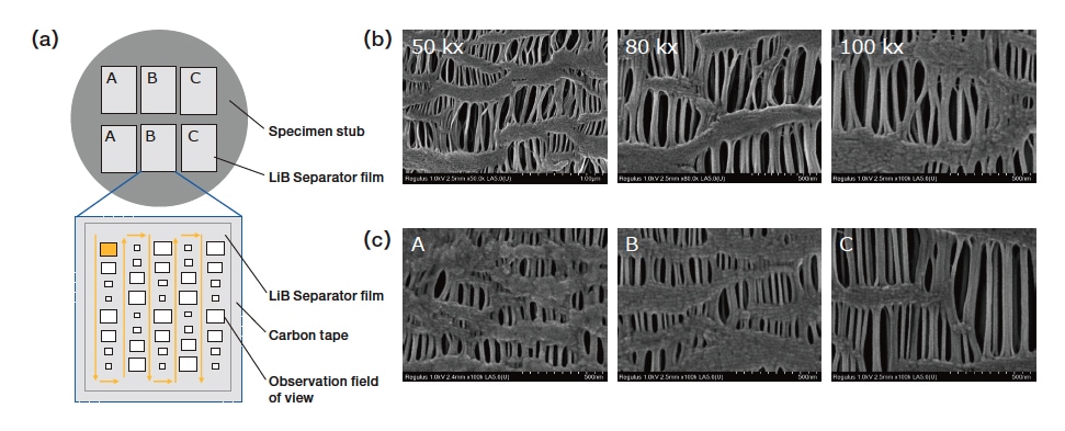
Fig. 3 Automated multi-specimen observation of LiB separators.
(a) Arrangement of specimens on specimen stub and sequence of automated observations.
(b) Secondary-electron images at magnifications of 50,000×, 80,000×, and 100,000×.
(c) Secondary-electron images at magnification of 100,000×.
(Instrument: Regulus8200. Accelerating voltage: 1 kV. Detector: Upper detector)
This observation targeted specimens of three LiB separator films (labeled A, B, and C) fabricated under different manufacturing conditions. As shown in Figure 3(a), two specimens of each separator were arranged on the microscope specimen stub; to minimize structural deformation and other variations during the automated procedure, the field of view was modified for each distinct observation magnification, as indicated by arrows in the figure. Figure 3(b) shows secondary-electron images at magnifications of 50,000×, 80,000×, and 100,000×, while Figure 3(c) compares secondary-electron images at 100,000× for specimens A, B, and C. The high-resolution observation yields insight into various factors governing ion transmissivity and other aspects of battery performance—including fiber width, pore size, and fine-grained surface roughness—while the ability to acquire large quantities of data with high stability allows direct comparison of the microscopic structures of the distinct separators.
Figure 4 shows an automated cross-sectional observation of semiconductor device patterns5). Pre-processing procedures to characterize semiconductor manufacturing processes require that various process steps be followed by SEM cross-sectional analysis of device patterns to measure dimensions and confirm shapes.
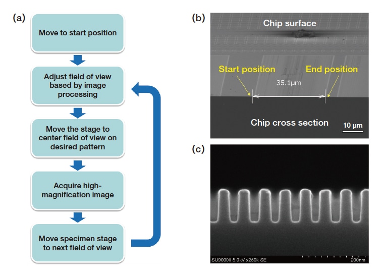
Fig. 4 Automated cross-sectional observation of semiconductor device patterns.
(a) Observation workflow. (b) Secondary-electron image at 800× magnification. (c) Secondary-electron image at 250,000× magnification.
(Instrument: SU9000 II. Accelerating voltage: 5 kV. Detector: Upper detector.)
In this observation, a region of approximate width 35μm [Figure 4(b)] was sequentially observed at 250,000× magnification to reveal the shapes of the microscopic patterns created within this region [Figure 4(c)]. Before each image was acquired, image-recognition techniques were used to center the observation field of view on the pattern in question; including the time required for this field-of-view calibration, the overall observation acquired a total of 56 images in approximately 15 minutes, roughly the same amount of time that would be required to capture an equivalent dataset via manual operation.
Figure 5 shows an automated observation of an electrode-gap sensor used to measure viruses. As depicted in Figure 5(a), this sensor consists of two electrodes, separated by a 10-μm gap, atop a Si substrate; the device functions as a biosensor for measuring viruses trapped in the gap between electrodes. The goal of this SEM observation was to acquire sequential images of the electrode-gap region to estimate the volume of virus material actually present within the sensor.
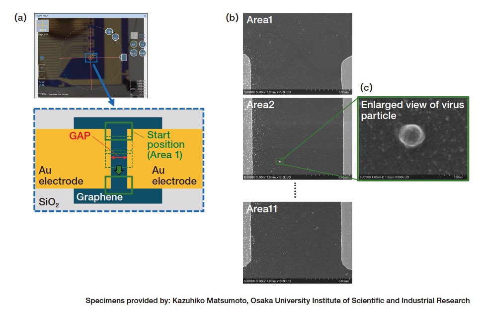
Fig. 5 Automated observation of electrode-gap sensor for virus measurement.
(a) Optical microscope image and schematic diagram of electrode gap. (b) Secondary-electron image at 10,000× magnification.
(c) Secondary-electron image at 300,000× magnification.
(Instrument: SU8600. Accelerating voltage: 3 kV. Detector: Upper detector.)
This observation began by reading a list of coordinates specified for the electrode gap, then moving the specimen stage to the vicinity of the electrode edge. Next, image-recognition techniques were used to adjust the field of view to ensure that the gap between electrodes was accurately captured; the resulting position was taken as the starting position for a sequence of images capturing the full electrode gap [Figure 5(a)]. After capturing one electrode-gap image, the field of view moved to the next position and image acquisition was repeated. Figure 5(b) shows a sequentially-acquired secondary-electron image at 10,000× magnification, while Figure 5(c) shows a manually-acquired secondary-electron image at 300,000× magnification of a virus present in the space between electrodes. This observation required images to be acquired at 11 fields of view for each of 30 electrode-gap locations, yielding a total of 330 observation fields of view; the automation procedure saved 2.5 hours of manual labor that would be required to acquire the same data by hand.
In this article we presented a series of practical case studies illustrating the use of EM Flow Creator to automate SEM observation workflows. These examples demonstrate the flexibility of EM Flow Creator in automating many types of observations, allowing large quantities of data to be acquired automatically through highly stable operational sequences—and reducing operational burdens on instrument users to streamline data acquisition and analysis.
References
About the authors
Takashi Shidara
Solutions Development Department
Beam Technology & Analytical System Products Division
Core Technology & Solutions Business Group
Hitachi High-Tech Corporation
See more
