
Hiroyuki Shinada
PhD (Engineering)
Technology Advisor
Research and Development Group
Hitachi, Ltd.
We are living through an era of rapid progress in the capabilities of AI engines and other digital technologies. These tools already can generate convincing drawings, photographs, or movies in response to written instructions, and can translate foreign languages into natural-sounding speech or text essentially in real time. These technologies have also begun to transform the field of electron microscopy, where the use of advanced digital techniques has become commonplace and has enabled sophisticated new achievements that would have been unthinkable in previous eras. This latter development comes as somewhat jarring to those of us who have been working in the field for some time. Indeed, when I began studying scanning electron microscopy (SEM) in the mid-1980s, the use of image-processing techniques to improve SEM image quality was widely considered somewhat taboo: not strictly prohibited, but considered appropriate only in certain specific cases. After all, in those days we had no choice but to print SEM images on film or specialized types of paper, so the line separating "authentic" SEM images from image-processed data was clear and unmistakable. Of course, even "authentic" SEM images are produced by electrons interacting with fields or material bodies and being transformed on the basis of physical law, so perhaps no essential difference between "authentic" SEM images and post-processed images is exist. In today's world, it seems entirely natural to apply advanced digital processing techniques to microscope images, thereby dramatically improving both the quality and quantity of measured data. Since 2010 I have been involved in developing an ultra-high-voltage holography electron microscope and in the years following the completion of this instrument I began working on applications of digital processing techniques to electron microscopy, and I will begin this article with a brief summary of these projects.
Electron holography is a technique that exploits interference between electrons to measure phase shifts experienced by electrons passing through electromagnetic fields, thereby mapping electromagnetic field distributions both inside and outside material bodies with the high spatial resolution of electron microscopy. Holography was invented by Dénes Gábor in 1948 to improve the resolution of electron microscopes. Its first practical implementations came in the optical domain, while for electron microscopes the first practical instrument was developed by Akira Tonomura in 1978. Tonomura went on to achieve a number of breakthroughs, including experimental confirmation of the Aharonov-Bohm effect and direct observation of magnetic flux quanta. In 2000, he developed a holography electron microscope with an accelerating voltage of 1 MV and successfully used it to observe the quantization of magnetic flux quanta in high-temperature superconductors. Later, he began developing an aberration-corrected holography electron microscope with an accelerating voltage of 1.2 MV for the purpose of observing magnetic-field distributions with atomic resolution (Figure 1), but tragically passed away before completing this work. I too participated in this development project, and after much hard work, the instrument was completed in 2014, after which we began using it as a tool for mapping electromagnetic fields with world-leading atomic resolution—with applications including analyzing electron devices and elucidating the mechanisms responsible for advanced functional properties in highly functional materials. Researchers pursuing R&D efforts in these areas have long lists of demanding requirements for metrological systems. In our efforts to meet these needs, we have attempted to combine and exploit the latest digital technologies—including machine learning, experimental automation, and large-scale data processing, all areas that have witnessed extraordinary advances in recent years—to transcend conventional limitations on instrument performance.
Since 2016 we have been supported by the JST Strategic Basic Research Program (CREST) grant in the "Intelligent Measurement Analysis" domain: our project, entitled "Advanced Electron Microscopy with the Aid of Artificial Intelligence and Image Processing (JPMJCR1664)," is a collaboration between Hitachi, Kyushu University, and the University of Osaka, led by Kyushu University Professor Yasukazu Murakami. In what follows we present examples of results achieved by our collaboration using our 1.2 MV ultra-high-voltage electron microscope.
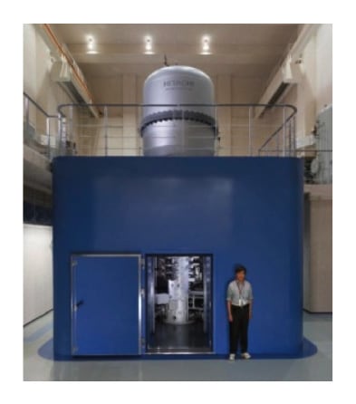
Fig. 1 Ultra-high resolution, high-stability, aberration-corrected holography electron microscope with accelerating voltage of 1.2 MV. The development of this instrument was supported by the Funding Program for World-Leading Innovative R&D on Science and Technology (FIRST) through a grant from the Japan Society for the Promotion of Science.
The phase shifts experienced by electrons traversing magnetic fields in miniscule regions such as atomic monolayers are extremely small—so tiny, in fact, that achieving the goals of the 1.2 MV holography electron microscope requires not only high spatial resolution, but also a high signal-to-noise ratio. To this end, we developed a technique for automatically acquiring large numbers of images (at present, up to approximately 10000) over a period of several days, then combining these images to yield data with a high signal-to-noise ratio. Of course, in automated data-acquisition runs spanning long periods of time, drifts in operating conditions—including instrument focus and aberration correction—are more or less inevitable. However, we have used a digital aberration-correction technique (Figure 2) 1,2), which processes images after acquisition to correct for any remaining aberration caused by such drifts, to minimize the associated degradation in image resolution. With this approach, we succeeded in mapping the magnetic fields present in individual crystal lattice planes—that is, the magnetic-field distribution within a single atomic monolayer—with a spatial resolution of 0.47 nm (Figure 3) 2). Incidentally, it is interesting to note that the idea of correcting aberration in images after their acquisition was Dénes Gábor's original motivation for inventing electron holography. Thus, this example demonstrates how advances in digital technologies have finally allowed electron holography to achieve its original founding goals.
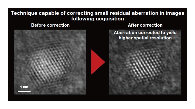
Fig. 2 An example demonstrating the use of digital aberration-correction techniques: Applying digital processing algorithms to images following data acquisition allows small residual aberrations to be corrected.
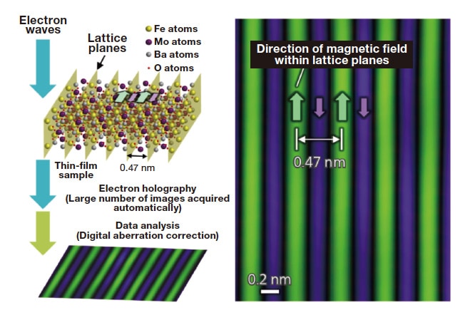
Fig. 3 Experimental observation of magnetic-field distributions within (111) lattice planes in a magnetic body (Ba2FeMoO6 crystal). Left: Schematic diagram of observational setup. Right: Measured data indicating that the magnetic field changes in magnitude and direction from one atomic monolayer to the next.
Catalysts capable of promoting various chemical reactions are important materials that help address many challenges, including environmental degradation, resource depletion, and energy creation. Understanding the properties of catalysts requires high-sensitivity mapping of the ultra-small electric fields that surround catalyst nanoparticles and affect their chemical reactions—a challenge to which electron holography is ideally suited. The sensitivity of electromagnetic-field measurements can typically be enhanced by irradiating samples with brighter electron beams to increase the signal-to-noise ratio. However, catalysts tend to be highly susceptible to damage under electron-beam irradiation, and may cease to exhibit their original structure long before an adequate signal-to-noise ratio can be achieved. Instead, we introduce the notion of single-particle analysis, a concept that has found practical applications in the analysis of proteins. The basic strategy is to acquire large numbers of images of a single type of catalyst, and then superpose them to yield a final image with a high signal-to-noise ratio. However, because catalysts exhibit a complex distribution of morphologies, we need a method for efficiently selecting catalyst particles of similar shapes and acquiring data only for these particles. To this end, we developed a technique that uses machine-learning algorithms to search automatically for desired fields of view. Given a large number of candidate catalyst nanoparticles, our algorithm efficiently selects particles that can be imaged with high resolution, then combines and averages multiple images to increase the signal-to-noise ratio. We also apply a version of the newly-developed numerical statistical technique known as wavelet-based hidden Markov models to reduce noise even further. The result of these innovations is to improve the signal-to-noise ratio for electric-field measurements by approximately tenfold compared to conventional approaches, allowing accurate detection of electron phase shifts indicating the presence or absence of a single electron (corresponding to approximately 1/1000 the wavelength of a 1.2 MeV electron). Using this technique, we succeeded in quantitatively mapping ultra-small electric fields around catalyst nanoparticles (Figure 4) 3).
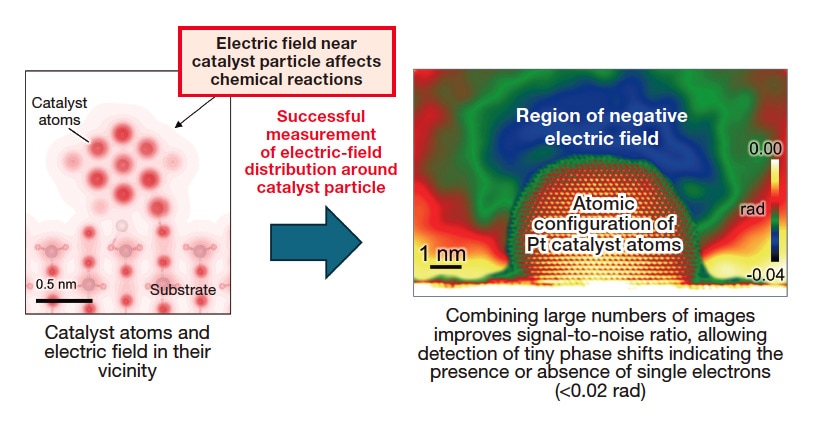
Fig. 4 Electric fields surrounding a catalyst nanoparticle. Colors indicate electric-field-induced electronic phase shifts. The measurement reveals a region above a Pt catalyst nanoparticle in which the electric field is negative.
The basic technique underlying the case studies we have presented may be described as the use of digital technologies to transform infinitesimal quantities of information, present in measured data, into features in images that may be discerned by visual inspection. Speaking personally, even as someone with a rather elderly brain, I have no trouble accepting these images without any sense of foreignness or artificiality. Taking things one step further, one might say that the information content of raw data offers little more than hints that must be related to enormous stockpiles of previously accumulated data and insights to interpret measured data. Indeed, the work recognized by the 2024 Nobel Prize in Chemistry demonstrated that AI tools could predict new protein structures—for which there exist no measured data—based solely on existing data and insights. For those of us who can remember a time when the use of image-processing techniques to improve the quality of SEM images was considered taboo, these developments may feel somewhat shocking and unsettling—and yet so very promising that we look forward in eager anticipation to watching them advance in years to come.
References
