Semiconductors that contribute to achieving a sustainable society
Nano-Technology Solutions ×
SEMI Japan
Right: Tetsuya Shigetomi General Manager Service Planning Dept. Digital Service Div. Nano-Technology Solution Business Group Hitachi High-Tech Corporation
The Road to a One-Trillion-Dollar Market — A Society and Economy Driven by Semiconductors
Shigetomi The semiconductor market is now one of the fastest-growing industries in the world. At Hitachi High-Tech, we offer a lineup of semiconductor manufacturing process products such as CD-SEM, plasma etching system, and defect/foreign matter inspection and analytical systems. But what role do semiconductors play in modern society?
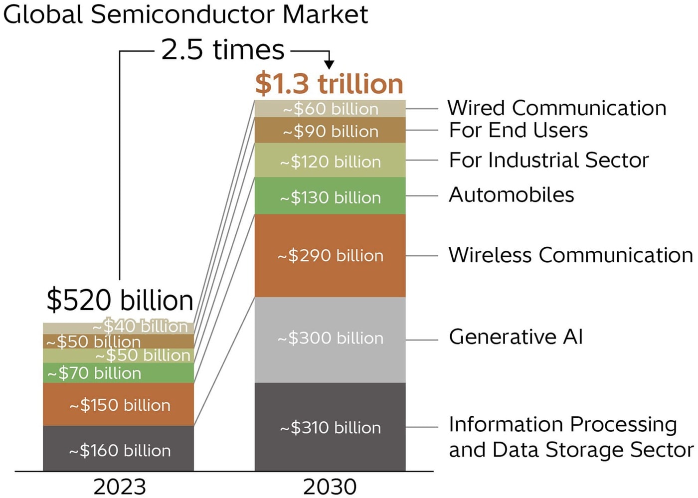
Eda Semiconductors are truly the core technology that supports today's social infrastructure. They are used in all products that support our daily lives, from smartphones and computers to automobiles and medical devices, making major contributions to quality of life improvement. Furthermore, they form the foundation that supports the advancement of cutting-edge technologies such as AI, quantum computers, and IoT, and are essential for accelerating innovation. The scale of the semiconductor market has reached about $520 billion over 50 years, but in just a few years, by 2030, it is expected to exceed $1 trillion in market growth. This accelerated growth indicates that the entire industry is rapidly shifting to the very core of society and the economy.

The Forefront of Sustainability in the Semiconductor Industry — Scope 3 and Current Industry Collaboration
Shigetomi On the other hand, to achieve a sustainable society, there are many challenges that the entire semiconductor industry must address. Amid such circumstances, as an industry leader, what initiatives is SEMI promoting?
Eda As a global semiconductor industry organization, SEMI supports industry development from various angles, including policy recommendations to governments, talent development, and strengthening collaboration across the entire value chain. We believe that our particular strength is providing a platform for non-competitive areas that address common issues beyond corporate competition. To achieve a sustainable society, under the SEMI Sustainability Initiative, each company participates in voluntary working groups set for each theme, cooperating with one another.
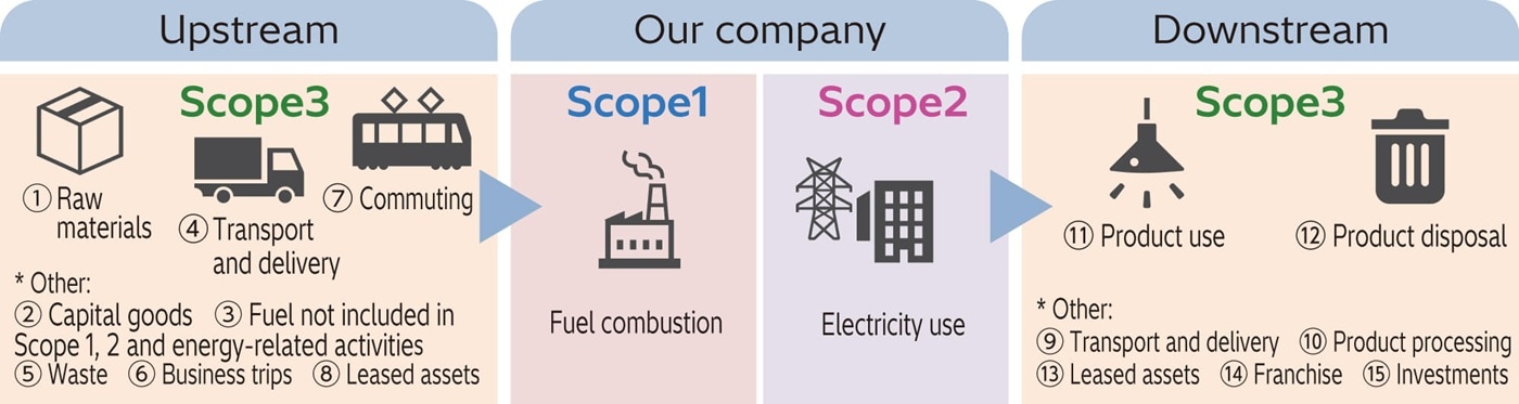
Representative themes include responses to regulations such as PFAS, ESG (environmental, social, and governance), and climate change, and we address challenges that are difficult for companies to tackle alone. Among these, the issue we place the most emphasis on is addressing climate change. In November 2022, SEMI launched the SCC (Semiconductor Climate Consortium). Within the SCC, the entire industry examines and implements effective reduction measures across all Scope 1–3*¹ emission categories to reduce greenhouse gas emissions across the entire value chain.
*1Supply chain emissions. When companies consider CO2 emissions, they calculate their own as Scope 1 and Scope 2, and the activities upstream and downstream in the supply chain as Scope 3. Scope 3 is classified into 15 categories.
Source: Green Value Chain Platform
With robust growth in semiconductor demand, the market is expected to reach $1.3 trillion by 2030.
Shigetomi At our company, addressing climate change is also one of our key initiatives. Aiming for net zero by 2050, we are working to reduce greenhouse gas emissions across the entire value chain.
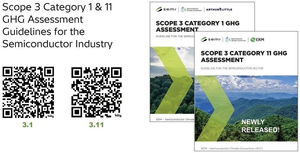
Eda To reduce greenhouse gas emissions, a response that looks at the entire value chain is required. As you know, although there is a cross-industry international standard called the GHG Protocol for calculating Scope 3 emissions, there has not been a guideline that meets the unique needs of the semiconductor industry in actual operations. Therefore, led by the Scope 3 WG (Scope 3 Working Group), we have promoted information sharing and issue identification in the semiconductor value chain, and recently published guidelines for calculating Scope 3 Category 1 (emissions from purchased products/ services) as well as Category 11 (emissions from the use phase of sold products). The aim is to supplement existing guidelines, protocols, and best practices. By providing guidelines tailored to the semiconductor industry, it seems that alignment of perspectives among companies is gradually advancing.
Shigetomi Hitachi High-Tech is also paying close attention to the activities of the Scope 3 WG. We see the establishment of industry guidelines as a significant step forward. Scope 3 accounts for the majority of our CO2 emissions, with about 90% coming from Category 1 and Category 11 in particular. Therefore, reducing these emissions is an important challenge.
For Category 1, we use CO2 emissions data supplied by our procurement partners for the products and services provided to us in our calculations. Visualizing emissions not only reflects each company’s initiatives, but also helps us plan our own reduction strategies. We have also started sending out e-mail newsletters to provide information on environmental regulations and other related topics. This supports the activities of procurement partners who do not have enough time to gather information. For Category 11, to reduce CO2 emissions during product use, we assess our environmental impact across the entire product life cycle, and through eco-design (environmentally conscious design)*² and life cycle assessment (LCA)*³, CO2 emissions reduction and resource circulation are promoted. In addition, by responding digitally to customers’ challenges, we are achieving shorter development times and higher productivity, contributing to lowering our environmental impact in semiconductor development and manufacturing.
*2A design method that identifies and assesses factors that impact the environment at every stage of a product’s life cycle, from raw material extraction to disposal, and incorporates measures to reduce our environmental impact.
*3A method for quantitatively assessing our environmental impact at each stage of the product life cycle by comparing the use of the developed product and conventional products.
Toward a Future Where We’re Glad to Be in the Semiconductor Industry — Fulfilling Our Responsibilities for the Environment and Society
Eda Going forward, I feel that industry-wide collaboration will become even more important. For example, we are working on developing calculation methods for PCF (Product Carbon Footprint) and systems to exchange emissions data smoothly across the supply chain. If information independently collected by each company can be shared in a common format, it will not only improve industry-wide efficiency but also make it easier to launch specific actions toward reduction.
Shigetomi I see. Standardizing formats will make it easier for our procurement partners to organize and submit information, reducing their operational workload. As a result, it may allow for more proactive cooperation than ever before.
Eda Visualizing and working to reduce our environmental impact is not something that can be accomplished by a single company alone. Precisely because this is a non-competitive area, I believe it is important for the entire industry to pool its expertise and move forward, supporting one another. Connecting each company’s efforts to the momentum of the entire industry—that's the role we hope to play.
Shigetomi As members of the semiconductor industry, let’s fulfill our responsibilities toward the environment and society, while recognizing that semiconductors are contributing to people’s lives and the advancement of society—and that we are all playing a part toward achieving this. Let’s work together to create a future that makes us feel, ‘I’m truly glad to be part of this industry,’ and proud to share that with our families and friends.
SEMI Japan Forest Initiatives
Since 2023, SEMI has been promoting a global tree-planting project called SEMI Forest. This is an initiative for supporting tree planting online for about $1 per tree, and it is also being developed in Japan as the SEMI Japan Forest. The current number of trees planted in the SEMI Japan Forest is 28,150. When converted to CO2 absorption, it is about 20 tons, which is equivalent to the annual CO2 emissions from six to seven manufacturing plants handling 300 mm wafers. More than just companies and organizations, invididuals are also able to participate starting from 25 trees. Of course, this is noted as part of corporate ESG activities and climate change responses, but it is also attracting attention as an easy way for anyone to get involved in sustainability.