
Ph.D. in Engineering
Associate Professor
Faculty of Engineering
Kyushu University
Tsuyohiko Fujigaya
In recent years, hollow metallic nanoparticles have attracted intense interest for their many remarkable properties, including giant specific surface area, catalytic activity, and low specific mass. Among their many applications are catalysts, sensors, energy-storage devices, molecular sieves, and batteries.1) To date, spherical nanoparticles,2) nanocubes,3) nanorods,4) and nanowires5) have been used as hollow metallic host nanoparticles. Nanowires are particularly promising host materials due to factors such as their strong adhesion to substrates and the ease with which they form network structures. Real-world applications of hollow nanowires include high-rate capacitors,6) solar cells,7) water purifiers,8) hydrogen producers,9) and catalysts.10)
One method of producing hollow nanowires is the template approach, which is capable of fabricating “barcode” nanowires with a periodic pore structure.11,12) In this method, electrochemical plating is carried out within a template in order to deposit a laminated structure containing two different metals: the metal that should be retained in the final structure (M1 in Fig. 1), and a sacrificial metal that is eventually dissolved to yield hollow regions (M2 in Fig. 1). Other reported fabrication techniques include those based on the Kirkendall effect13) and on galvano-substitution reactions.14) In all cases, precise control of the diameter and length of the host material, and of the hollow regions are important for obtaining the desired properties. In the present study, a structural characterization of such nanowires was performed by ultra-high resolution scanning electron microscopy (SEM) using a Hitachi High-Tech SU9000. Because the SU9000 allows—in addition to high-resolution SEM imaging—the acquisition of transmission images, dark-field images, and X-ray fluorescence (energy-dispersive X-ray spectroscopy) images within the same field of view, it is an extremely powerful instrument for investigating the exterior and interior of barcode nanowires, in additional to performing elemental analysis. In the experiments reported here, the full power of this instrument is demonstrated.
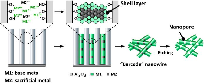
Fig.1 Procedure for fabricating hollow barcode nanowires
In the present study, the template method combined with electrochemical plating was used to fabricate nickel (Ni) /silver (Ag) barcode nanowires. The Ag layers were treated as sacrifi cial, and were dissolved to produce nanowires with a periodic pore structure. The nanowires were formed within uniformly wide channels in anodic aluminum oxide (AAO),15) as illustrated in Fig. 1. An advantage of this process is that because the diameter and length of the AAO channels can be controlled based on the anodic oxidation conditions and the thickness of the initial aluminum foil, the dimensions of the nanowires can also be controlled.
To fabricate the nanowires, 200 nm of Ag was first evaporated onto the surface of an AAO film with a pore size of 18 nm to serve as an electrode for electrochemical plating. The plating bath consisted of an aqueous solution containing 685 mMNiSO4·6H2O as a Ni source, and 0.577 mM Ag2SO4 as a Ag source. Plating was performed using a three-terminal cell: the working electrode was the Ag-covered AAO fi lm, the counter electrode was Pt, and the reference electrode was Ag/AgCl. Voltages of -0.4 and -1.0 V (relative to the Ag/AgCl electrode) were applied to alternately deposit Ag and Ni, respectively. This process relies on the fact that, at -1.0 V, both Ag and Ni undergo a reduction reaction and plate the surface; this allows a highly excessive quantity (1,000×) of nickel to be introduced into the plating bath to minimize the impact of Ag contamination in the Ni layer.16)
The electrochemical plating conditions were as follows. A programmable potentiostat (Hokuto Denko HZ-5000) was used to apply alternating voltages of -0.4 V for 120 s and -1.0 V for 10 s (Fig. 2A). The AAO film was then dissolved using a 1.0 M sodium hydroxide solution. Figure 2B shows a dark-field scanning transmission electron microscopy (STEM) image of the resulting metallic wire. The wire length was uniform and the thickness was roughly the same as the AAO pore size (18 nm). Figure 2C shows EDX line profiles along the length of a single nanowire. It can be seen that the signal intensity due to Ni (blue) alternates with that due to Ag (pink), indicating successful laminated Ni/Ag plating. This is confirmed by the EDX elemental maps in Fig. 2D, in which alternating blue and pink bands are clearly seen. The corresponding dark-field STEM image is also shown in the figure, but the two types of regions are essentially indistinguishable. As shown in Fig. 2E, the SU9000 allows EDX elemental mapping with even higher resolution. Interestingly, an EDX signal due to Ni was detected in the Ag region.
This demonstrates that the SU9000 is capable of performing EDX mapping at the same high resolution as STEM imaging, thus offering an extremely effective method for identifying the structure of barcode nanowires. In the present study, Ni-Ag barcode nanowires were successfully fabricated for the first time. However, similar structures were previously reported for Fe-Au,17) Co-Cu,16) Co-Pt,18) Ni-Cu,19) and Ni-Pt.20) We encourage interested readers to consult these references for further details.
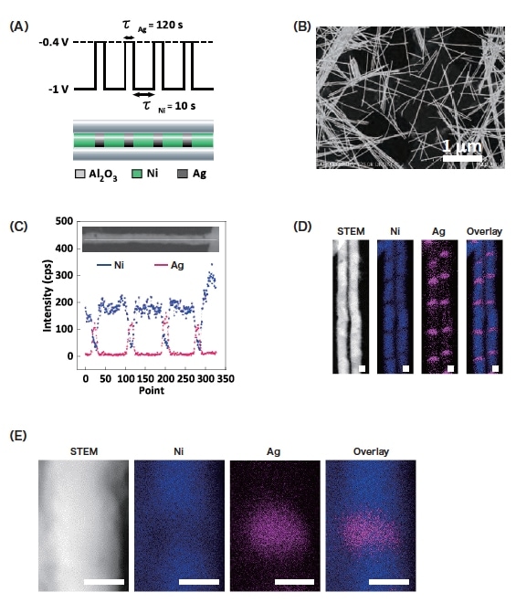
Fig. 2 (A) Schematic depiction of applied voltage waveform (top) and corresponding barcode nanowire structure (bottom).
(B) STEM image of barcode nanowire.
(C) EDX line profile for single barcode nanowire. Nickel and silver are shown as blue and pink, respectively.
(D, E) Images of Ni-Ag barcode nanowire: STEM image, Ni mapping image, Ag mapping image, overlay of Ni and Ag mapping images. Scale bar: 10 nm.
The Ni-Ag barcode nanowires were next processed in an ethanol solution of hydrogen peroxide and ammonia to dissolve the sacrificial silver layers. As is clear from the dark-field STEM images shown in Figs. 3A and 3B, the resulting nanowires contained joint-like regions and resembled bamboo shoots. Although it was initially expected that dissolution of the Ag would cause the nickel regions to separate from each other, yielding nanorods, the nanowires mainly retained their original length. From the dark-field STEM images, the lengths of the Ni and joint regions were estimated to be 75 ± 9.1 and 12 ± 5.3 nm, respectively, which are in complete agreement with the thicknesses of the original Ni and Ag layers. Thus, it does not seem to be the case that the interconnections are formed by residual Ag regions. Indeed, in the EDX line profiles in Fig. 3C, almost no Ag is detected. We therefore concluded that the joint regions were interconnected by some other mechanism. By exploiting the high-resolution capability of the SU9000, the joint regions were observed at high magnification. As shown in Fig. 3D, the results indicated that the Ag layers do not form cylindrical pillars as expected, but have a cylindrical shell structure with Ni forming the shell. We believe this explains the presence of the small amount of Ni in the Ag layer shown in Fig. 2E. The presence of a shell-like Ni layer with no remaining Ag is also confirmed by the EDX profiles in Fig. 3D. It can therefore be concluded that the hollow nanowire structure is the result of interconnections between nickel regions at the wire surface. A similar result was also obtained for AAO films with a larger pore size of 35 nm, demonstrating that this is not an effect of pore diameter.
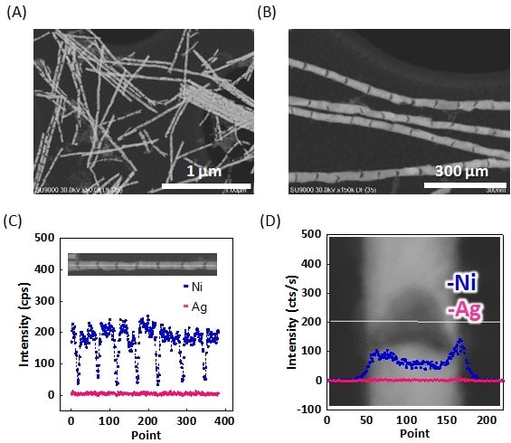
Fig. 3 (A, B) Dark-field STEM images of barcode nanowires after dissolution of silver.
(C, D) EDX line profiles for single barcode nanowire after dissolution of silver. Nickel and silver are shown in blue and pink, respectively.
We suggest that the reason for the formation of this type of nickel shell layer is the segregation of nickel ions near the inner walls of the AAO channels due to an interaction between Ni ions and OH groups on the AAO inner walls.21) Indeed, in experiments in which the AAO was immersed for 30 s in either a 0.2 M Ni-ion solution or a 0.2 M Ag-ion solution, and inductively coupled plasma - mass spectroscopy (ICP-MS) measurements were conducted to quantify the amount of adsorbed ions, the concentration of Ni was found to be three times higher than that of Ag, indicating more Ni was adsorbed than Ag. This is not surprising since the plating bath used in the electrochemical plating process was adjusted to contain Ni ions at a concentration 1,000 times greater than that of Ag ions.
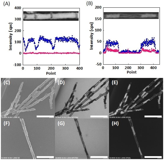
Fig. 4 (A, B) EDX line profiles for single hollow Ni barcode nanowire. In both cases, Ni and Ag are indicated by blue and pink, respectively.
(C-H) Images of hollow nickel barcode nanowires: SEM images (C,F), bright-field STEM images (D,G), dark-field STEM images (E,H). Scale bar: 200 nm.
One of the advantages of this alternating plating technique is that the length of each layer can be precisely controlled by varying parameters such as the duration of the applied potential and the bath concentration. Figure 4A shows bright-field STEM images and EDX line profiles for hollow Ni barcode nanowires fabricated with a Ag plating time of 120 s and Ni plating times of 5, 10, and 15 s. Analysis of these figures reveals Ni-layer lengths of 38 ± 5.1, 79 ± 6.3, and 122 ± 11.4 nm, respectively, demonstrating successful control of the layer length. Figure 4B shows similar results for nanowires fabricated with a 10 times higher concentration of Ag ions (5.77 mM). The hollow regions are seen to be longer, demonstrating that the length can also be controlled by varying the concentration. An extremely interesting finding is that despite the expansion of the hollow regions, they remain connected by the Ni shell, indicating that the shell is uniformly thick.
Based on the discussion thus far, one might ask: Is SEM capability really necessary? Would it not be sufficient simply to combine STEM observations with EDX measurements? However, the use of SEM imaging allows visible confirmation of small voids like those shown in Figs. 4C and 4F. This is a crucial observation and offers the key to achieving future improvements in uniformity. In all cases, it seems that Ni segregation occurred uniformly at the inner walls of the AAO. Thus, largely for the purposes of demonstration, we fabricated Ag nanowires by electrolysis at a fi xed potential of -0.65 V; after dissolving the Ag, we successfully obtained hollow “nickel nanotubes,” as expected (Fig. 5A). From the high-resolution SEM images, bright-field STEM images, and dark-field STEM images shown in Fig. 5B, we can determine not only that the tubes are hollow, but also that their surfaces are not smooth, but have regions of adsorbed amorphous material.
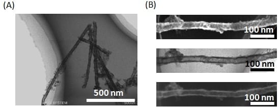
Fig.5 (A) Bright-field STEM image of nickel nanotubes.
(B) Images of nickel nanotube: high-resolution SEM image (top), bright-field STEM image (middle), dark-field STEM image (bottom).
Thus, the unexpected result of this study is that we have succeeded in establishing a technique for fabricating hollow nickel barcode nanowires.
The metallic barcode nanowires investigated in this study provide a clear illustration of the ability of the SU9000 to acquire both high-resolution scattered-electron and transmitted-electron images, and to perform high-resolution elemental mapping. By exploiting the power of this instrument, a clear understanding can be obtained of surface features and internal structure, together with the distribution of elements, this yielding a powerful tool for structural identification. Researchers continue to discover unique new ways to use these methods for research beyond the topics reported here. As just one example, for studies on metallic nanoparticles supported by graphene or a similar nanosheet, the techniques described in this report—specifically, the combination of scattered-electron and transmission-electron images—would allow the visual discrimination of particles supported between the front and back surfaces of the sheet.
References
See more
