
Takashi Sumigawa
Ph.D. (engineering)
Associate Professor
Department of Mechanical Engineering and Science
Graduate School of Engineering
Kyoto University
Investigations of the strength of materials tend to focus on mechanical tests involving materials of dimensions ranging from nanometers to micrometers. Among the main reasons for this are (1) the discovery of characteristic structures at the nanoscale, and (2) changes in mechanical properties associated with the miniaturization of structural materials. Examples of item (1) include constituent elements with characteristic dimensions and structures on the order of nanometers, typified by graphene, fullerenes, and carbon nanotubes. Although simulations have pointed out the extraordinarily high strength and other peculiar physical properties of these materials, ultimately, simulations are nothing more than predictions made on computers, and experimental demonstration is essential for establishing their validity. Structures of this type form in a bottom-up manner, and once a fabrication process has been established it is relatively easy to provide experimental samples1). Item (2) originated with the discovery that material metals shrunken to sizes on the order of micrometers or nanometers—such as ultra-miniature wire interconnects and circuit elements in semiconductor electronic devices—exhibit characteristic mechanical properties that differ significantly from those of macroscopic metals. A typical example is the case of yielding phenomena in metals, where the yield stress (in the single-crystal case) is approximately constant and size-independent for macroscopic materials, but increases with decreasing sample dimensions at scales on the order of micrometers or smaller2). Most experiments use specimens made from macroscopic materials—that is, prepared via top-down processes—and the methods used to prepare samples, as well as the experimental procedures used to study them, involve significant differences of technique and interpretation between researchers and engineers, with the result that the characteristic mechanical properties of nano-or micron-scale materials remain poorly understood.
In order to realize mechanical loading tests for specimens with dimensions ranging from nanometers to microns, focused ion beam (FIB) processing and scanning electron microscope (SEM) observation are of crucial importance. In this paper, after first discussing the roles played by FIB and SEM in experiments to characterize the mechanical properties of ultra-miniature specimens fabricated via top-down processes, we present a case study from our research group: tension-compression experiments conducted inside an SEM with in-situ observation.
"Smaller is stronger" has been a well-established tenets for the mechanical strength of materials. For example, in the interior of glasses and ceramics there exist micron-scale defects, invisible to the naked eye. As the dimensions of a material sample get smaller, the probability that the sample will contain fatal defects (defects responsible for the breakdown of the material) decreases as well, increasing the material strength. In addition, for metallic materials it has been reported that the yield stress increases for samples of sizes on the order of micrometers or below. In this phenomenon, a key role is played by "dislocations", which govern the plastic-deformation properties of a material; this phenomenon associated with shrinking sample dimensions is brought about by a reduction in the number of initial dislocations, fewer dislocation sources, shorter dislocation sources, geometrically necessary dislocations, and greater influence exerted by free surfaces and interfaces with other materials. Material-strength research affects a wide range of fields. For example, high-temperature and environmental properties are expected to exhibit unusual and characteristic dependence on sample dimensions as sample are miniaturized into the microscale or nanoscale regime.
Specimens used in mechanical experiments to examine the dependence on sample dimensions in the microscale and nanoscale regimes are often prepared by FIB. Other methods, such as photolithography and dry etching, are used in some cases, but FIB has the advantages of being able to process various materials and of offering considerable freedom in choosing the desired shape of the processed sample. On the other hand, one drawback is that the gallium-ion beam used in FIB leaves behind a damage layer on the processed surface; as the thickness of this layer is typically a few tens of nanometers, it can have significant influence on the mechanical properties of microscale and nanoscale specimens.
Figure 1(a) shows the results of transmission-electron microscope (TEM) observations (bright-field image) of the vicinity of the processed surface of a sample of annealed copper (Cu, purity 99.999%), with the processing carried out using an FB-2200 (accelerating voltage 40 kV, current 10 pA or below). For this type of processing, we use a beam parallel to the surface being processed. The TEM image shows that a damage layer, of thickness several tens of nanometers, is left near the free surface. Our research group attempted to eliminate processed layers from specimens by argon (Ar) ion milling using the Gentle Mill Hi3). Figure 1(b) shows a TEM image of a Cu sample subjected to Ar ion-milling (accelerating voltage 0.5 kV) after FIB processing. Note that the procedure successfully removed the damage layer introduced by the FIB. For silicon (Si), it has been reported that damage layers introduced by FIB processing can be removed by the application of a thermal treatment after the FIB step4-5).
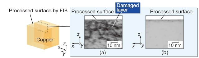
Fig. 1 TEM images of the vicinity of a processed Cu surface (a) after FIB, (b) after FIB + Ar milling3)
When fabricating ultra-miniature specimens, proper handling of samples is of the utmost importance, and the FB-2200 is equipped with features that are suitable for this purpose: a microsampling mechanism and local vapor-deposition capabilities. Figure 2 shows a fabrication process developed by our research group for on-chip assembly of specimens3). In this case the components of the specimen consist of a single-crystal gold (Au) nanorod—the object of the measurement—installed at the center of a diamond-shaped Si frame; pressing the upper portion of the frame allows a tension load to be applied to the nanorod. The microsampling mechanism and local vapor-deposition apparatus are used both to extract Si and Au ultra-miniature materials—prepared from macroscopic materials via FIB—and to install the Au component in the Si frame. Note that, of the two components of our specimen, the milling rate for Au is higher than that for Si, and thus when we perform Ar ion milling using a broad beam after FIB processing, so that essentially only the Au component is affected.
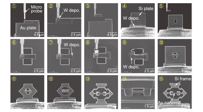
Fig. 2 On-chip assembly of the components of a specimen consisting of an Au nanorod and a Si frame
Needless to say, microscale and nanoscale specimens cannot be seen directly by the naked eye; to observe specimens and the damage they suffer we must use an electron microscope. In particular, when investigating material deformation and failure phenomena it is important to make successive observations (in-situ observations) throughout the course of the process, whereupon the experiment must be conducted inside an SEM or a TEM system. Because electron microscopes have only limited capacity to accommodate equipment within their sample chambers, we are forced to prepare a custom-designed ultra-miniature loading test device. Our group owns in-lens (S-5500), semi-in-lens (SU8230), and out-lens (SU5000) field emission-SEM (FE-SEM) instruments; the choice of which instrument to use depends on the purposes of the experiment and the observation. The in-lens FE-SEM has high imaging resolution of below 1 nm, but uses a sample holder similar to that used for TEM observations, which limits the dimensions of the samples that can be observed to a few millimeters. For this reason, the size of the test instrument that can be accommodated is restricted to just the volume of the holder tip. In contrast, the out-lens instrument has the advantage of accommodating specimens with dimensions as large as 10 to 20 centimeters, but the imaging resolution is not as high as that for the others. Figures 3(a), 3(b), and 3(c) show the apparatuses we use for in-situ-observation load tests in the S-5500, SU8230, and SU5000 respectively. The apparatus in Figure 3(a) is equipped with a piezo-actuator at the tip of the S-5500 holder, allowing indentation tests during in-situ observations. The load is applied by a diamond indenter equipped with a special-purpose load sensor constructed using micro-electro-mechanical system (MEMS) techniques. The apparatus in Figure 3(b)-1 is equipped with a stage capable of translational motion in three orthogonal directions, while that in Figure 3(b)-2 is equipped with a stage allowing rotation about 2 axes. These tools allow high-precision, high-resolution load tests and in-situ observations to be conducted inside the SU8230. The apparatus in Figure 3(c) includes a stage with 6 degrees of freedom of motion (translational motion in 3 orthogonal directions and rotation about 3 axes); it is also equipped with a specially-developed slider for multi-layered piezo actuators, a gripping mechanism, and many other sophisticated special-purpose structures. The desiderata of high capacity to accommodate test instruments (the larger the instrument, the less restrictive its design tolerances and the more sophisticated the features that may be built into it) runs counter to that of high observation resolution. Therefore, one must choose the optimal tool for the objective in question.
Figure 4(a) shows the results of S-5500 observations of an Au single-crystal specimen of sub-micron dimensions subjected to repeated loading6). The images allow detailed observation of the damaged region, which consists of crystallographic plates, approximately 15 nm in width, separated by nano-cracks with a width of a few nanometers. Figure 4(b) is an in-situ observation7) of a tension test conducted inside the SU8230; the subject of the test was a Si nanospring fabricated by the dynamic oblique deposition method. The instrument succeeds in capturing clear images of the Si nanospring and remains largely unaffected by charge-up by electrons.
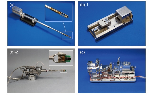
Fig. 3 (a) Test apparatus used with the S-5500 (developed exclusively for Nanofactory), (b) test apparatus used with the SU8230 (1. Hysitron PI85, 2. Kleindiek micromanipulator), (c) test apparatus used with the SU5000 (custom-developed)
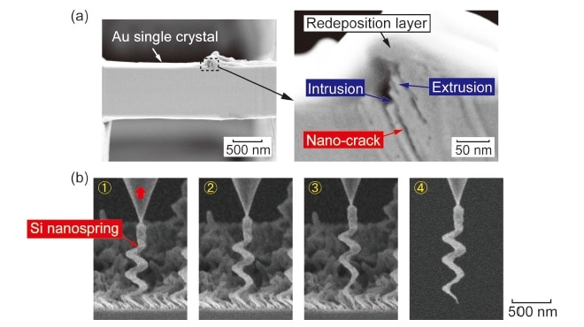
Fig. 4 (a) Fatigue-damaged region of a sub-micron sample of single-crystal Au, as observed by the S-55006), (b) in-situ observation of tension test of Si nanospring conducted inside the SU82307)
As most failures in metallic structures are traced to causes originating in fatigue, detailed mechanisms for this behavior have been clarified. For example, cyclic loading with a plastic strain load on the order of 0.01–0.1% to Cu gives rise to a localized deformation region, characteristic of fatigue phenomena, known as a persistent slip band (PSB). The interior of PSBs contains fatigue dislocation structures formed by the self-organization of dislocations into ladder-like structure with widths on the order of 1 µm, which in turn produce regions of similar width on material surfaces exhibiting roughness features known as extrusions/intrusions9). The characteristic 1 µm length scale of these structures is determined by the elastic strain field of individual dislocations; it is an intrinsic property that is not affected by sample dimensions. PSBs cause deformation mismatches at matrix interfaces and concentrations of stress at intrusion roots; they govern material failure due to fatigue by serving as preferential initiation sites and propagation pathways for fatigue cracks. On the other hand, this also implies that, when a material sample itself has dimensions on the order of micrometers or nanometers in all directions, the fatigue structures cannot be formed in the interior of the material and the phenomenon of fatigue-induced failure does not arise. However, the truth or falsity of this prediction remains unclear.
Due to the inherent difficulty of the experiments, to date there have been essentially no reports of cyclic loading tests to characterize the mechanical properties of samples with microscale or nanoscale extents in all three dimensions. Even if we extend consideration to the full range of experiments for evaluating material strength, only one-directional loading tests have been performed; on top of this, in most experiments a simple compression deformation is applied to samples.
In recent years, from the reason of the simplicity of loading style, a few bending deformation tests have been reported. However, these studies cannot elucidate the pure and basic nature of fatigue phenomena of microscale or nanoscale materials owing to the presence of stress gradients within bent samples because stress gradient induces the sample-size dependence of fatigue phenomena. To resolve this problem, it is essential to conduct tension-compression tests, which do not give rise to stress gradients in materials. Motivated by this background, our research group took on the challenge of tension-compression testing inside a SEM with in-situ observation.
After applying a heat treatment to a polycrystalline Cu plate under a vacuum, coarsening crystal grains, and eliminating residual stress, we used electron backscatter diffraction (EBSD) to obtain crystal-structure information for the plate surfaces. From a grain which has desired crystal orientation, we fabricated ultra-miniature specimens by FIB. The specimen possesses I-type shape consisting of a base section, the test section, and a grip section [Figure 5(a)]. Surface damage layers introduced by FIB processing were removed via Ar ion milling. Figure 5(b) shows a stereograph indicating the crystal orientation of the specimen and the Schmid factors corresponding to the 12 slip systems for Cu. The specimen had a single slip direction in which one slip system was preferentially active; in the figure, the primary slip system with the largest resolved shear stress is labeled B4 (the combination of slip plane B and slip direction 4). Also, we defined the side walls of the test region to be Side 1–Side 4 [Figure 5(c)]. For this specimen, the height of the region through which slips due to the primary slip system pass is approximately 400 nm.
We used a Hysitron PI85 to conduct tension-compression loading tests inside the SU8230. We used FIB to form the diamond loading chip of the apparatus into the shape of a hook, and then used this hook to capture the grip section of the specimen to realize tension-compression loading [Figure 5(d)].
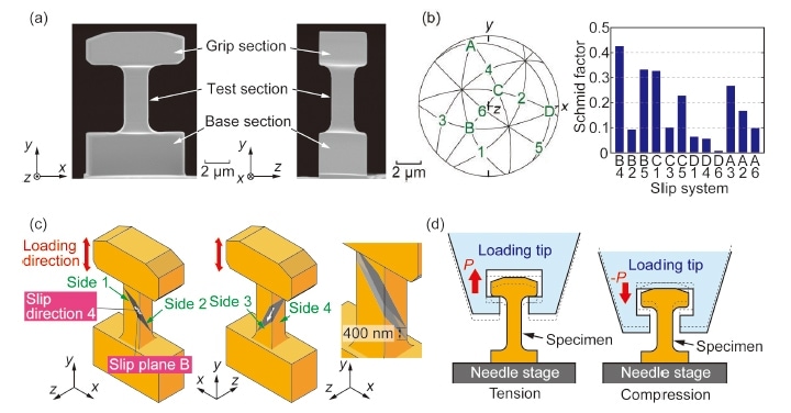
Fig. 5 (a) Micro-Cu single-crystal specimen, (b) stereograph indicating the orientation of the specimen and Schmid factors, (c) schematic diagram of the primary slip system, (d) method for achieving tension-compression loading8)
In the tension-compression test (strain amplitude: 7.5×10⁻²) a fatigue crack arose on the 7th cycle. Figure 6 shows (a) an in-situ SEM image during the first cycle, and (b) the stress-strain relationship. During the first half cycle in which a tension load was applied, the specimen initially exhibited elastic deformation, then showed yielding in the vicinity of τ=56 MPa (point B in the figure).
Thereafter, upon arriving at τ=82 MPa (point C in the figure), the sample became unstable and exhibited a rapid increase in strain (strain burst). We note that this value of the yield stress is approximately 100 times greater than that for the bulk material (approximately 0.5 MPa10)). In images observed at the end of the tension loading, fine slip lines emerged across a wide area of the test region. In the remaining half cycle (compression loading), the specimen initially exhibited elastic deformation behavior, then showed yielding at τ=-31 MPa (point E in the figure). Thus, the specimen exhibited a Bauschinger effect: the phenomenon of decreasing yield stress in the reverse deformation. Subsequently, in conjunction with cyclic work hardening, the specimen repeatedly executed a cycle of rapidly increasing displacement amplitude and rapidly decreasing load amplitude, with an enormous strain burst at τ=-75 MPa (point G in the figure) on the compressive side.
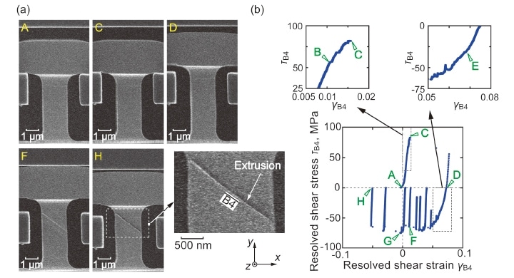
Fig. 6 (a) FE-SEM images during the test (taken on the first cycle), (b) relationship between resolved shear stress and resolved shear strain8)
Figure 7 shows FE-SEM images of the specimen, captured at the end of every half cycle using the SU8230 at low scan speed. Due to the strain burst under tension loading during the first cycle [Figure 7(a)], fine slip lines appear across the entire test section, while under compression loading [Figure 7(b)], we see local slip concentration [the emergence of extrusion]. As is evident from the deformations in the 2nd and subsequent cycles, this local deformation is irreversible. As the number of cycles increases, local slips result in the growth and elongation of nanometer-scale extrusions and intrusions, and ultimately a crack emerges from the base of the intrusion.
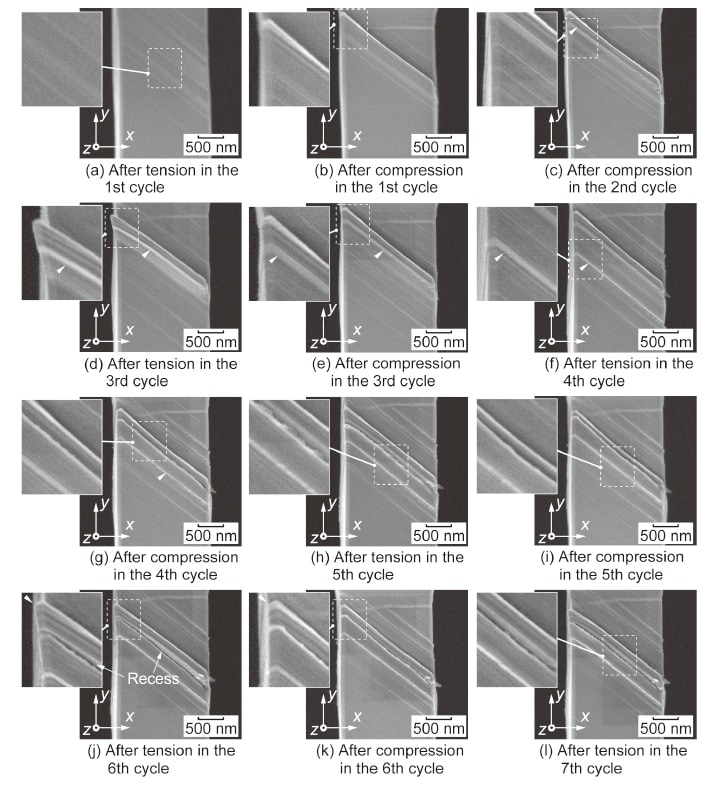
Fig. 7 FE-SEM images (observed using SU8230) captured at the conclusion of every half cycle8)
The images shown in Figure 8 are the results of observations made with the S-5500 of specimens after the test. Crystallographic plates of thickness 100-300 nm run through the test section along the primary slip system B4. On Side 1 and Side 3, extrusions/intrusions form with heights in the range 170-430 nm. These extrusions/intrusions bear a superficial resemblance to those observed on the surfaces of bulk Cu (with widths around 1 µm), but they are vastly narrower in width, and an extrusion on one surface corresponds to an intrusion on the opposite surface. By the 7th cycle, a crack has emerged from an intrusion with a sharp angle.
By testing with in-situ observations, we were able to determine that gaps (extrusions) appear locally during the compression-loading phase of the first cycle, and that the extrusions/intrusions responsible for the emergence of fatigue cracks are formed by the repeated deformations of several cycles. The mechanism for this formation is clearly distinct from that underlying extrusions/intrusions for bulk Cu, which form on the specimen surface in conjunction with the self-assembly of dislocations in the interior of the material. Moreover, if strain with an amplitude comparable to that used in these tests was applied to bulk Cu (single-crystal), multiple slips would result, with fatigue cracks arising from collisions between slip bands and macroscopic deformation bands that cross them; for the specimen used in our experiment, in contrast, planar slips governed deformation up to the emergence of cracks, which first appeared at the base of intrusions. Thus, our results clearly indicate the significant differences between the mechanisms responsible for the formation of fatigue defects in microscopic and macroscopic material specimens.
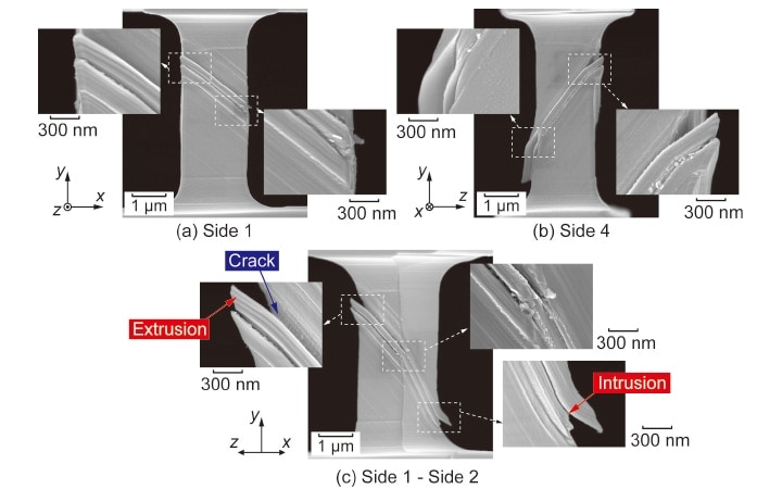
Fig. 8 SEM images after fatigue test (observed using S-5500)8)
In this paper, we introduced a method of tension-compression cyclic testing with in-situ observation and applied it to an investigation of micro-Cu single crystals to demonstrate its utility in characterizing the mechanical properties of ultra-miniature material samples. Improved understanding of the mechanisms of fatigue in ultra-miniature materials will lead to an enormous advance not only in academic research but also in the industrial world. In fatigue phenomena, cracks initiate primarily from the material surface, and thus surface treatments (to eliminate processed layers when fabricating specimens) and in-situ observations during tests are particularly important. This is why FIB techniques, the surface treatments associated with them, and SEM observations all play roles of enormous significance. Moreover, accurate characterization of the mechanical properties of microscale and nanoscale materials is relevant not only for an understanding of material strength, but has become increasingly necessary throughout a wide range of fields for studies of electrical properties, mechanical responses to ferroelectricity, and other phenomena. We have every expectation that the demand for mechanical testing with in-situ observation inside electron microscopes will grow only more urgent in the years to come.
References
See more
