
Masaaki Sugiyama
Ph.D. (Engineering)
Specially Appointed Professor
Graduate School of Engineering
Osaka University
When subjected to changing temperatures, metallic materials—much more than semiconductor or polymeric materials—undergo a broad diversity of structural transformations, exhibiting phenomena ranging from precipitation to phase transformations and even element partition among the phases at high temperatures. The ability to control the dynamical structure changes in consideration of mechanical and functional properties creates several kinds of values for the production of practically useful industrial materials. However, experimental tests of characterization techniques for controlling structural changes are typically conducted at room temperature, leaving few options for studying structural changes at high temperature. Most studies attempt either to quench high-temperature structures by rapid cooling to room temperature or to pursue empirical control schemes informed by predictions from computational models. This has spurred intense interest in the possibility of using in-situ observational methods to make direct measurements of structural changes at high temperatures—a prospect discussed by the Japanese Society of Microscopy in a survey of current challenges and future directions for scanning electron microscope (SEM) 1). However, in electron microscopy, samples are observed in a vacuum. Observations under ambient pressure using optical microscopes or similar instruments are difficult due to problems caused by oxidation—and, in practice, have been further complicated by a variety of technical problems, such as detectors themselves failing to withstand high temperatures. Considering the situation, it is noted that high-temperature in-situ observation has not yet achieved the status of a general-purpose analytical technique suitable for arbitrary applications.
Meanwhile, dramatic recent progress in techniques for analyzing material structure, coupled with advances in computational methods that allow highly realistic modeling of high-temperature structural changes, have created strong demand for direct dynamical insight—both experimental and computational—into the structural consequences of material heating. In this environment, the method of SEM—which can not only accommodate relatively large size samples, but can also serve as a self-contained mini-laboratory capable of recreating macroscopic phenomena on mesoscopic length scales—has once again emerged to play a key role in the multi-scale microstructure analysis. In particular, with modern SEM technology it is now easy to measure crystal orientations in polycrystalline metallic materials. This has enabled advances such as the use of the sample-heating electron backscatter diffraction stage to observe temperature-induced changes in the crystal phases of a sample mounted in an SEM system2) and the installation of a large biaxial tensile tester to study the deformation of metals3). The development of SEM techniques for in-situ observations over extended time intervals has also been eagerly anticipated for studies of semiconductor bonding wires and in other fields4). All of these developments have spurred interest in questions such as the limits of the temperature range over which samples may be stably heated and the performance that may be expected from detectors at high temperatures.
Motivated by these developments, in this paper the application methods of a high-resolution draw-out SEM system for in-situ observations of heated samples are discussed. There is a variety of SEM results and discuss a number of relevant issues, including the feasibility of elemental mapping at high temperatures5).
Transforming an SEM system into a mini-laboratory requires two essential components: (1) a draw-out mechanism for exchanging samples, and (2) a Schottky electron gun for high spatial resolution. The SU5000 SEM system from Hitachi High-Tech satisfies these requirements—and is designed to accommodate sample-heating stages and a variety of other types of sample stage. This instrument also extends the capabilities of conventional SEM systems— instruments which excel at imaging three-dimensional structural features—to allow the time evolution of threedimensional structural features to be observed in real time. Figure 1 shows the SU5000 system and the Gatan Murano sample-heating stage, which the SU5000 supports.
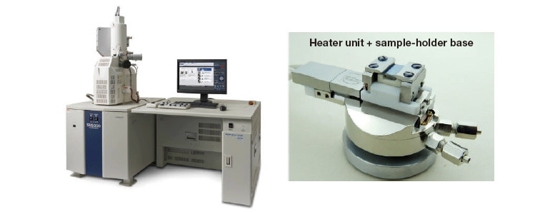
Fig. 1 The SU5000 scanning electron microscope system (left) and the Murano from Gatan Inc. (right), a sample-heating stage supported by the SU5000.
First, to investigate experimental conditions for in-situ observation of heated samples, we make measurements using Ametek’s EDAX Octane silicon-nitride SDD detector [Figure 2(a)], which is equipped with a highly heat-resistant SiN window and a filter for use with heated samples. This yields the results shown in Figure 2(b); note that, even at 950°C, it is succeeded to measure the EDS spectrum of Fe with no peak shifts. By way of contrast, Figure 3 shows the results of measurements made with a conventional EDS detector at 900°C; comparing the initial measurement (left) to a measurement made some time later (right), it is seen that the position of the Fe EDS peak shifts toward higher energies at later times. In these figures we have added dashed vertical lines at 1 keV and 6 keV to emphasize the shift in the apparent characteristic X-ray energy for Fe. This shift is caused to fluorescence from the Fe sample upon heating to high temperatures inside the SEM. Of course, such shifts are not problematic for materials whose composition is known in advance. However, for detecting EDS spectra from materials that exhibit precipitation, phase decomposition, or similar phenomena upon heating, it is essential to design a system in which these shifts do not occur.
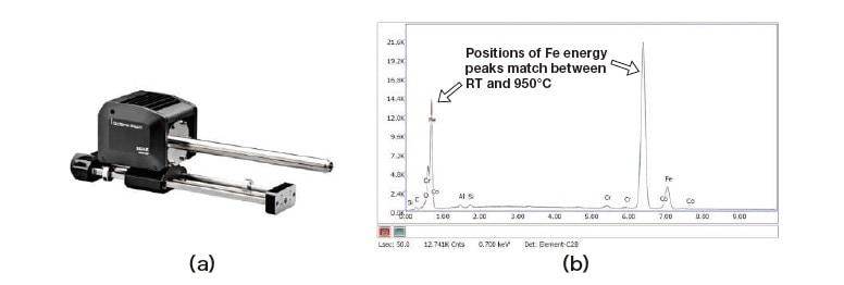
Fig. 2 (a) EDAX silicon-nitride SDD detector from Ametek. (b) EDS profiles for Fe sample measured at room temperature and at 950°C.
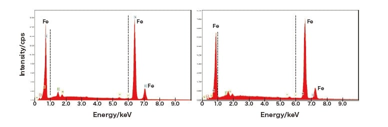
Fig. 3 Positions of Fe spectral lines in measurements made at 900°C using general-purpose (conventional) EDS detector.
For these experiments SUS304 stainless steel is utilized, which is an austenite-structured alloy that does not exhibit phase transitions during the heat treatment. The composition of this material is the standard Fe-0.06C-18Cr-8Ni (where numerals indicate wt%). At temperatures in the range 450-850°C, it has long been known that SUS304 exhibits precipitation of the carbides M23C6 (where M stands for Cr or Fe, with Cr the primary species) at austenite grain boundaries, accompanied by the formation of Cr-depleted layers at adjacent sites (a phenomenon known as sensitization) 6). In particular, the reduction in Cr concentration near grain boundaries tends to degrade the high corrosion resistance for which stainless steel is named. In view of this, it is important to investigate the precipitation and corresponding diffusion behavior of Cr element at high-temperature7). In particular, although the formation of Cr-depleted layers accompanying sensitization has been addressed by many studies, a number of points remain to be clarified, including the behavior in the low-temperature regime below 500°C. It is also reported from another point of view that a study involving SUS304 subjected to a sensitization treatment of 100 h at 700°C discovered the emergence of two distinct isothermal martensitic transformations, one occurring near grain boundaries and the other occurring in grain interiors8). Since the same sample is used for this study, the characteristic isothermal martensitic transformation will be investigated using the stable heating stage under SEM observations in near future.
Figure 4 shows an example of structural change induced by sample heating inside the SEM system. For this observation we used an accelerating voltage of 20 kV and a WD of approximately 10 mm, and acquired secondary electron images at a magnification of 2,000×. The sample was first heated stepwise from room temperature to 600°C at an average rate of 50°C/min, then held temporarily at 600°C for measurement and observation, after which heating resumed as before. At temperatures up to 600°C there is essentially no drift in the secondary electron image, indicating that the sample-heating stage furnishes a stable sample environment at these temperatures. Evidence for structural change begins to emerge near 600°C in the form of indentations observed at grain boundaries. Discrete dark pointlike regions begin to emerge clearly near austenite grain boundaries at 650°C [Figure 4(c)]. In Figures 4(c,d) arrows indicate twin boundaries, which are known to occur frequently in FCC crystals of austenite grains. Note that there is no sign of any structural change near these twin interfaces, in comparison with the interface such as a grain boundary. In the 750°C image the indentations showing black contrast at grain boundaries have grown larger with increasing of temperature, suggesting that the formation of Cr carbides and the emergence of Cr-depleted regions are in progress at this point. It was previously reported that the production of carbides near crystal grain boundaries proceeds more rapidly when the crystal structures on each side of the boundary are mismatched or misaligned; this suggests that, contrarily, carbide production should be occurred at only grain boundaries instead of twin boundaries with wellmatched crystals, as shown in the figure. In this experiment the sample was heated from room temperature to 600°C in 12 min; based on the results of previous studies, it is considered that this relatively short interval is too brief to allow significant dispersion of Cr through the grain boundary of sample9). The significant change, nonetheless, of prominent dark-contrast regions near grain boundaries in Figure 4 indicates that a small change of the grain boundary structure already starts at 600°C, and alternative in-situ observational methods with higher spatial resolution will be expected.
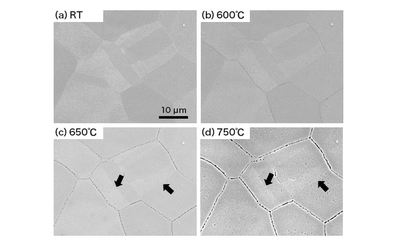
Fig. 4 Secondary electron images captured via in-situ observation of SUS304 sample heated during SEM observations. Arrows indicate twin boundaries.
In the secondary electron images dark contrast regions at grain boundaries always appear on heating in SEM; we now use three-dimensional observation methods to confirm that these are due to indentations in the sample surface. A convenient feature of the SU5000 system—which offers a variety of 3D measurement capabilities—is that it is equipped with a backscattered-electron detector whose target area is subdivided into 4 quadrants. By reconstructing image data from each quadrant, the system can create images representing bird’s-eye views of a sample’s surfaceroughness profile. As we have not tested the performance of this detector at high temperatures, we allow the heated sample to cool to room temperature before proceeding with our 3D observations. The resulting bird’s-eye image of surface roughness is shown in Figure 5(b); Figure 5(a) is the backscattered-electron image, and the left portion of Figure 5 is a schematic diagram illustrating the operation of the 4-quadrant detector. From the images, it is concluded that the depth of the surface indentations at grain boundaries is around 100-200 nm. Characterizing the accuracy of the detector and testing its performance at high temperatures are topics for future work.
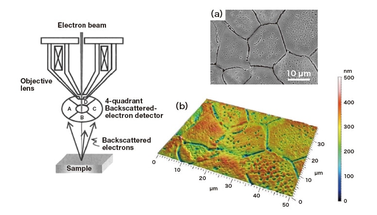
Fig. 5 Left: Schematic diagram of four-quadrant backscattered-electron detector. Right: Secondary electron image (a) and reconstructed image showing bird’s-eye view of roughness (b).
As noted above, the formation of Cr-depleted regions near grain boundaries in SUS304 significantly affects the material properties of the alloy—specifically, its corrosion resistance—and it seems likely that other interactions among constituent elements may be of similar relevance. We now show that EDS mapping of high-temperature samples, in combination with the other observational techniques we have discussed, yields fascinating insights into these phenomena. Figure 6 shows elemental mapping results obtained at 600°C, near the onset of structural transformation near grain boundaries. This observation required approximately 1 hour of measurement time using the drift-correction capabilities of the SU5000. In the secondary electron image in Figure 6(b), the regions of varying contrast indicated by arrows are twin boundaries. As noted above, we expect little or no structural change in such regions, and thus we focus on the spatially-varying distributions of element abundance near the austenite grain boundaries that meet at the triple point at the center of the images. Figures 6 (d), (e), and (f) respectively show elemental mapping results for O, Fe, and Cr. As is clear from these maps, many—though not all—of the grain boundaries in this material are distinguished by a prevalence of oxidation in their vicinities. Structurally, we observe the emergence of a region with distinct new features on the both sides of grain boundaries in Figure 6(c); the similarity between this image and the oxygen distribution map in Figure 6(d) suggests that the new material region may be due to the production of Cr oxides. Production of Fe-Cr-O oxides could, in principle, be a plausible alternative hypothesis, depending on the partial pressure of oxygen; however, the plot of Fe-rich regions in Figure 6(e) is nearly a photographic negative of the plot of O-rich regions in Figure 6(d), suggesting that Fe and O do not coexist and that Cr-O is the most likely candidate. Note that the prevalence of oxidation near grain boundaries is also affected by the orientation of the boundaries; for example, we find minimal production of oxides in the vicinity of the red-circled grain boundary in Figure 6(f). Indeed, the grain boundary appears to be rich in Cr, a fact which may be related to the production of M23C6 expected at grain boundaries. On the other hand, as seen in Figure 6(d), oxygen is detected even at Cr-rich grain boundaries, so there is no guarantee that the observation of Cr implies the presence of carbides. As is clear from the bird’s-eye view of the surface roughness in Figure 5, the large surface indentations near grain boundaries make these regions imperfect targets for EDS analysis, and the complete picture at high temperatures is too subtle to be captured in full detail information by simple methods of elemental analysis or structural observation.
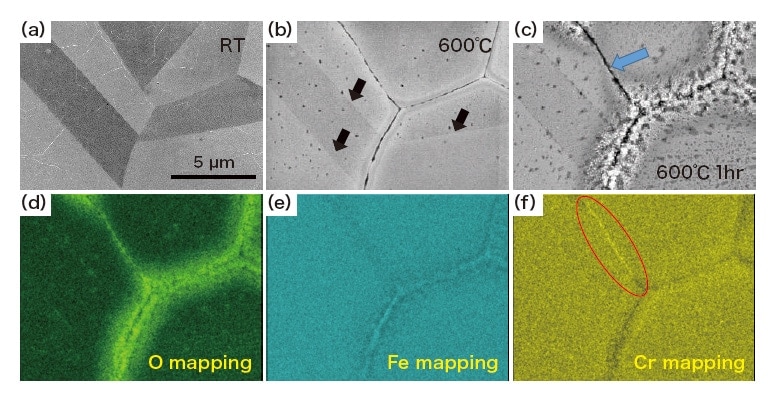
Fig. 6 (b,c): Secondary electron images acquired at 600°C. (d,e,f): Elemental mapping images for O, Fe, and Cr.
Thus far we have successfully demonstrated that the system for in-situ heating and observation easily accommodates structural-change and elemental-mapping experiments. However, the formation of oxides near grain boundaries is clearly influenced by factors such as residual oxygen in the SEM system and oxygen introduced into the system from the original sample before the observation. These factors will create serious problems when we attempt to establish a mini-laboratory inside the SEM system. Because the surface of the SUS304 base material was coated by a Cr-O-based passivating film, and because we did not perform any particular sample preprocessing before our experiments, we must consider the impact of oxygen introduced into the system by the sample. To this end, we next investigate the possibility of preprocessing samples via planar ion milling. The ion milling system we use is the ArBlade5000; Figure 7 shows a photo of this tool and a schematic diagram of its use. The present treatment condition is irradiated for 10 min at 4 kV, applied to all sample surfaces.
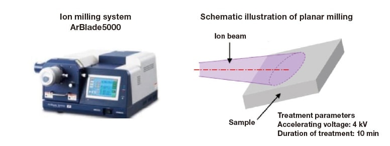
Fig. 7 Left: The ArBlade 5000 ion milling system. Right: Schematic diagram illustrating planar ion milling.
The results of in-situ observations of a treated sample are shown in Figure 8. No significant production of compound oxides observed near g rain boundaries at any temperature over the full range of 200-800°C. Although we have not tested retention over long time intervals, this suggests that the formation of the oxides observed in Figure 6 may be due to oxygen introduced to the system from the sample. Also, a comparison of the structures at 600°C indicates that indentations at grain boundaries develop at a slightly slower pace. At 800°C we observe the emergence of nonuniform surface-roughness profiles in grain-boundary regions, resulting in the possibility of the production of carbides. At higher temperatures, the dark contrast regions near grain boundaries disappear, suggesting some suppression of surface indentations near grain boundaries.

Fig. 8 In-situ observation of ion-milled SUS304 sample heated using SEM sample-heating stage.
The disappearance of discrete dark-contrast regions—including oxides—from grain boundaries is evident in Figure 9(a). Carbides produced by sensitization treatments are well known to reconstitute solid solutions in austenite following high-temperature solid-solution treatments, and thus we believe that this corresponds to the emergence of surface roughness due to precipitation of M23C6 particles produced non-uniformly at grain boundaries and the disappearance of non-uniformity due to the reemergence of solid solutions within grains. Austenite stainless steels are commonly subjected to homogenizing treatments at temperatures above 1,000°C. The in-situ observations at 950°C indicate that the positions of austenite grain boundaries began to move by significant distances, as shown in Figure 9(b). This shows that the characteristic grain boundary growth induced by high-temperature industrial treatments also leave clearly identifiable signatures observable by in-situ SEM. The sensitization and related phenomena—not only in heated samples, but also at normal temperatures in samples subjected to deformation stress tests—have been recognized as problematic ever since the earliest days10). From the perspective of establishing mini-laboratories within SEM systems, it is fascinating to wonder if new studies using modern techniques may finally yield solutions to these longstanding problems.
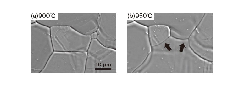
Fig. 9 Secondary electron images acquired by in-situ observation of crystal grain growth at high temperatures.
The SU5000 is a SEM system equipped with a high-resolution Schottky electron gun and a draw-out architecture to ensure a spacious instrument chassis capable of accommodating a wide variety of sample-mounting configurations. In this article we investigated some applications of one such configuration—namely, a sample-heating stage for in situ observation of materials at elevated temperatures. Austenite stainless steel is a typical material used for the large application fields such as heat resistance and corrosion resistance materials. However, in practical applications, this material—like various other industrial steel products—is known to suffer from the lack of strength of welding portion, corrosion susceptibility at high temperatures, and a great many other difficulties associated with diffusion and precipitation of Cr and other elements, resulting in the change of microscopic structure. For in-situ observations in the SEM, deviations from the actual conditions under which materials are used—including the temperature of the stage, the impact of residual gases, and the vacuum level in a SEM chamber—cause uncertainty for understanding the experimental results. However, recent advances in dynamic measurement techniques are creating advanced component technologies capable of solving these problems. The experiments reported here were made possible by many lending instruments from Hitachi High-Tech, creating a valuable opportunity to revisit the idea of building mini-laboratories inside SEM systems. The choice of the common material SUS304 for measurement samples enabled a variety of investigations regarding the experimental heating environment. We are hopeful that the catalog of experimental conditions we have compiled will prove valuable for future use in devising remedies for specific research problems.
Acknowledgements
For invaluable assistance in the completion of this study, including lending instruments of sample-heating stages and other equipment, we extend our deepest gratitude to T. Tani and K. Shigeto of Hitachi High-Tech Corporation. We are also grateful to M. Yamada of Ametek Inc. for assistance with the EDAX detector. This article is based on content previously presented at the 74th Annual Meeting of the Japanese Society of Microscopy in 2018.
References

See more
