Shigeaki Tachibana*1, William Podrazky*2
Scanning Electron Microscopes (SEM) are used for observation and analysis in various fields. Since Field Emission SEM (FE-SEM) equipped with a field emission electron gun source provide higher resolution than those equipped with a thermionic emission electron gun source, the user base for FE-SEM has broadened significantly due to the need to observe specimen features continually decreasing in size. FE-SEMs are increasingly recognized as a tool for performing various surface analyses, however detection technologies for various signals generated from specimens have advanced beyond topographic observation alone. Typically the operator must utilize previous knowledge, training, and skill in microscopy to generate desirable results; therefore, optimal performance may vary based on experience level.
For example, optimal performance may not be realized as a result of improper optical axis alignment or astigmatism correction, utilizing unsuitable accelerating voltage(s), or other parameters. Integrating an automated solution for these problems would allow the user to focus on obtaining comprehensive results under the best possible conditions at all times.
Hitachi High-Tech has developed a novel user interface which augments conventional SEM techniques to assist these problems. The "EM Wizard" user interface was developed to bring "new usability" to EM operators of various levels of experience. This Schottky FE-SEM, the SU5000, incorporated with EM Wizard interface, launched in August 2014 (Fig. 1).
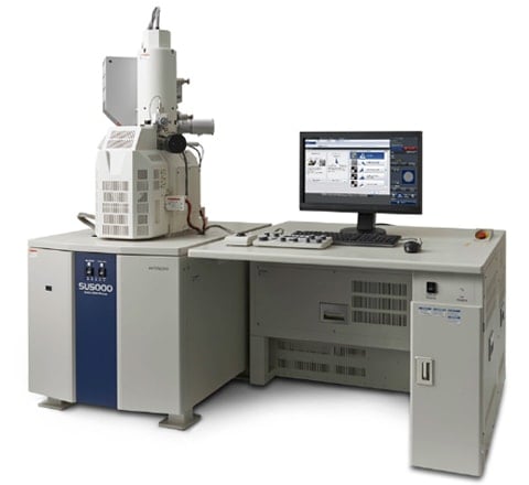
Fig. 1 External appearance of SU5000 FE-SEM
With EM Wizard, rather than setting individual conditions such as the accelerating voltage, working distance, detector, and other parameters, the operator can select an "Observation Purpose", such as "Surface Information" or "Elemental Information", from a selection menu (*2). On the screen, a Radar Chart displays the type of content that will be acquired (resolution, surface information, elemental composition), and a simulated SEM image representing how a specimen will appear under each observational objective. This information provides a visual understanding of SEM image characteristics that can guide the operator in selecting these objectives (Fig. 2).
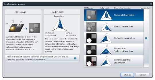
Fig. 2 EM Wizard, objectives selection screen.
When an "Observation Purpose" is selected, related system parameters are set automatically (e.g., accelerating voltage, working distance, detector), and optical axis parameters as well as astigmatism corrections are adjusted to optimal values. Simply by adjusting the brightness/contrast and focus, the operator can easily acquire high quality images at consistent resolution.
In addition to an applications selection menu, what makes these functions possible are high-precision automation technologies initially developed for Critical Dimension (CD) SEM. CD-SEM are entirely automated, and must provide highly reproducible measurements, optical axis alignments, and other adjustments; EM Wizard has been designed to use these automation technologies to reproduce and maintain highly precise adjustments invariably. Because optical axis alignment and astigmatism correction values change with lens conditions over time, they cannot be maintained for long periods, even if stored in the system. However, EM Wizard includes an auto-calibration function which automatically restores parameters to optimal values responsive to long-term changes in lens conditions (*3), eliminating any need for proficiency in readjustment procedures. This feature makes it easier for the operator to obtain images in focus, maintain high reproducibility, and acquire data efficiently.
Figure 3 is an example of a catalyst observed at 200,000x magnification after auto-calibration with the use of EM Wizard. Metal particles several nm in size are discernible during operation without complex adjustment.
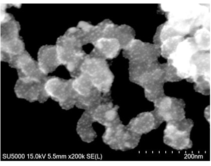
Fig. 3 Catalyst observation. Magnification: 200,000x
In addition to the assistance functions provided by automation as shown above, the SU5000 is equipped with optical and detection systems suitable for any variety of analysis required.
The emitter used is a Schottky-type device which delivers a spatial resolution of 2.0 nm at 1 kV (*4) and high probe current (>200 nA). Figure 4 is an example of the positive electrode of a lithium-ion battery observed at a landing voltage of 0.3 kV.
The positive electrode of Lithium ion batteries is comprised of an active substance consisting of conductors, binders, and other elements. However, some binder materials cannot withstand electron beam irradiation and must be observed at the lowest possible energy.
The left image in Fig. 4 was produced by a secondary electron detector mounted inside the electron column, and the right image was produced by a backscattered electron detector inserted below the lens. In the secondary electron image, the binder appears dark by voltage contrast, while the backscattered electron image allows for distribution of contrast based on each material. In this example, multiple signals are used to evaluate different components of the electrode including topographic and compositional distributions.
It is inferred that the enhanced voltage contrast in the secondary electron image is attributed to differences in the charge effect of each material due to the secondary electron generation efficiency when irradiated by very low-energy incident electrons.
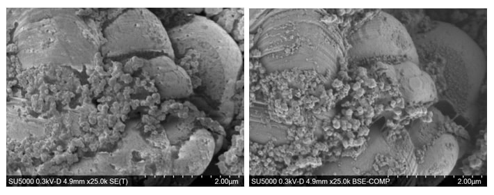
Fig. 4 Observation of lithium ion battery positive electrode.
Left: Secondary electron image. Right: Backscattered electron image. Magnification: 25,000x.
The SU5000 was developed to address the various needs of SEM users in materials science, biomedicine, and many other fields. As the FE-SEM grows in popularity, Hitachi will continually place importance on functions such as EM Wizard, which are capable of providing high-resolution and optimized contrast images with high reproducibility, regardless of the user experience level.
References
Sato M., History of Technologies in high resolution SEM, Kobunshi, 9 (2014)(Japanese).
Authors
See more
