Yasushi Kuroda*1, Yoshihisa Oishi*2, Ikuko Nakatani*3, Shota Torikawa*3
Focused ion beam (FIB) instruments are used for failure analysis in a wide variety of fields, ranging from semiconductor devices to metallurgy and ceramics. Recent years have seen an increasing demand for high-precision FIB analyses that require only short periods of time. In response, Hitachi High-Tech has been continuously engaged in the development of new FIB instruments—exploiting programmable processing and continuously automated processing based on our own unique technologies—that achieve dramatic increases in analytical efficiency and enable extremely high-level analyses that can be completed quickly. In recent years, there have also been increasingly active efforts to characterize the size and distribution of cores of defects caused by foreign substances in failure analyses, gathering information on their three-dimensional dispersion within the sample. Three-dimensional analytical techniques using hybrid FIB-SEM instruments have been widely adopted as means to achieve these goals. The MI4050 focused ion beam system from Hitachi High-Tech (Fig. 1) is equipped with a Cut&See feature that allows automated three-dimensional analysis. Because this instrument allows observations via a scanning ion microscope (SIM), it can be used to obtain clear images even for samples susceptible to channeling or charge accumulation (Fig. 2). In this report, we describe the Cut&See feature of the MI4050 and discuss a number of sample applications.
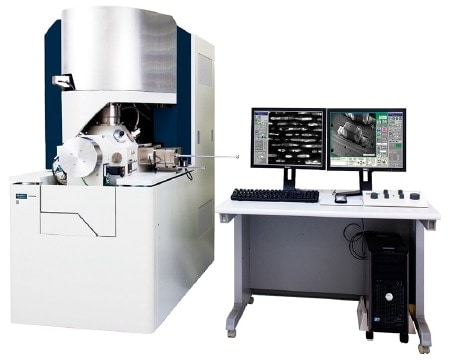
Fig.1 Focused Ion Beam system MI4050.
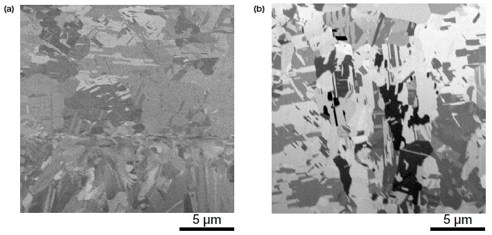
Fig.2 Comparison of (a) SEM and (b) SIM images of copper-foil interconnects on a printed circuit board.
(a) Accelerating voltage 3 kV, magnification 4,000×.
(b) Accelerating voltage 30 kV, FOV 20 µm.
Cut&See is a method of three-dimensional analysis in which FIB processing and observations are repeatedly performed in sequence. In conventional FIB instruments, the FIB processing, stage tilting, and cross-sectional analysis must be repeatedly performed by hand. In contrast, the automated Cut&See feature of the MI4050 allows automated repetition of the sequential procedure constituting the following processing flow: process slice, tilt stage, correct for observation position, capture cross-sectional SIM images, reset stage tilt, and correct for processing position. Because stage tilting is done in the eucentric position, there is essentially no shift between the processing and observation positions. The stage allows tilting up to a maximum of 60 degrees, and a total of two images may be captured for each slice—for example, one low-magnification and one high-magnification image, or one secondary-electron image and one secondary-ion image—yielding a maximum total of 1,000 image captures. The thickness in the FIB processing steps may be set to values in the range of 1 nm-1 µm.
Other key specifications of the MI4050 are listed in Table 1.
| Accelerating voltage | 1.0-30 kV, 0.5-30 kV* |
|---|---|
| SIM Resolution | 4 nm @ 30 kV |
| Maximum beam current | 90 nA or higher |
| Maximum beam current density | 50 A/cm2 |
| Detectors | Secondary electron detector, secondary ion detector* |
| Sample stage | 5-axis motorized eucentric tiling stage |
| Sample size | 50 (W) × 50 (D) × 12 (H) mm |
*Optional
In this section, we apply the automated Cut&See feature to the three-dimensional processing of copper-foil interconnects on a printed circuit board.
Figure 3 shows continuous FIB image slices of copper-foil interconnects on a printed circuit board. Thanks to channeling contrast, we are able to make SIM observations in which the crystal orientation of the copper-foil interconnect is clearly reflected in the light/dark pattern of the images. We see that the direction of the FIB-processed cross section is not sensitive to crystal orientation.
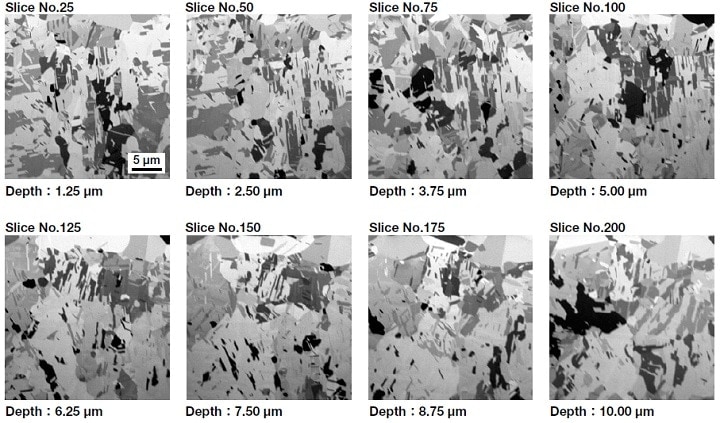
Fig.3 Continuous FIB image slices of copper-foil interconnects on a printed circuit board.
Processing condition:
•Accelerating voltage: 30 kV; Beam current: 12 nA; Size of processed sample: 20×20×10 µm
•Processing steps: 50 nm; Number of slices: 200
Observation condition:
•Accelerating voltage: 30 kV; Beam current: 100 pA; Signal detected: SIM image
Figure 4 shows the results of a three-dimensional reconstruction of the continuous image slices. Here we have used a false color display for the light/dark crystal regions. Looking at the sizes and distributions of the green, blue, pink, and purple regions corresponding to the four types of crystals, we see that the crystal sizes range from approximately 1 µm to 10 µm and are present in roughly identical proportions.
Based on these findings, we conclude that the combination of SIM images based on channeling contrast and flat processing via FIB offers promise for applications to performance evaluation of surface-mount components.
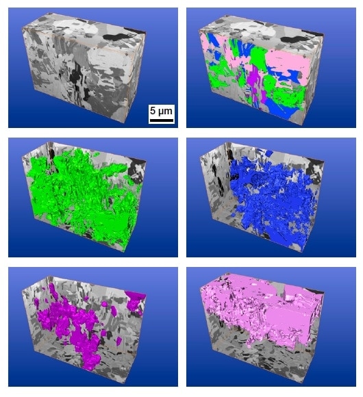
Fig.4 Three-dimensional reconstructions of continuous image slices of copper-foil interconnect on a printed circuit board.
In this report, we have discussed the Cut&See feature, which allows easy and automated three-dimensional analysis using a single-beam FIB instrument. Given the increasing demand for high-precision and high-efficiency analytical techniques, we expect that this instrument will play important roles not only through its core functionality but also in combination with programmed processing and automated processing methods.
References
Authors
See more
