A cutting-edge SEM instrument with a more compact footprint
Hiroyuki Komuro* Mari Sakaue**
Scanning electron microscopy (SEM), which is used to evaluate the microscopic morphology of specimens, has become essential for research and development in various areas of research, including metals, minerals, ceramics, cements, glasses, plastics, rubbers, petroleum products, paints, semiconductors, electronic components, and biomedical sciences.
SEM allows observations of the microstructure of specimen surfaces from low to high magnifications, and the depth of focus in SEM is larger than that in optical microscopy, which makes it easy to clarify the structure of an entire specimen with large surface roughness. An additional feature of SEM is X-ray analysis, which can be used to analyze the elemental composition in microscopic regions of specimens. Moreover, under low-vacuum conditions, SEM makes it possible to observe and analyze insulators and water- or oil-containing specimens without preprocessing. Therefore, SEM can be used in various applications, ranging from life sciences and foodstuffs to quality control for electronic components, for which SEM instruments have enjoyed increasingly broad adoption in recent years. The idea of low-vacuum observations was utilized to develop tabletop SEM instruments that can be used as an extension of optical microscopes. These instruments are controlled by a graphical user interface (GUI), similar to compact digital cameras, are capable of being directly operated by a novice user, and can easily capture high-magnification images beyond the reach of optical microscopy.
We have developed the FlexSEM 1000, a high-performance compact instrument that combines the miniaturization techniques underlying these tabletop microscopes with conventional high-performance SEM technology, and introduce it in this report.
Figure 1 shows an external view of the FlexSEM 1000. To accommodate various customer installation requirements, we have separated the main unit from the power supply unit, allowing the FlexSEM 1000 to be installed either as a tabletop unit or in a standalone configuration. To achieve this, we have miniaturized the instrument's electron-optical unit, which is responsible for the SEM performance, as much as possible while retaining the capability for high-resolution imaging. We have optimized the vacuum system by equipping the instrument with both a high-vacuum mode and a low-vacuum mode.
We have reduced the size and weight of all of these control systems.
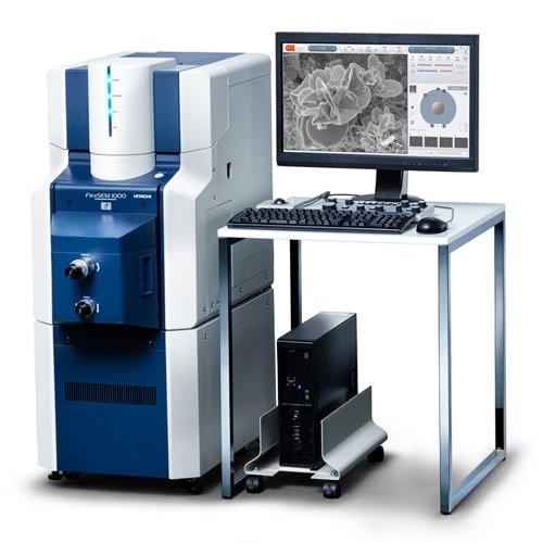
Fig 1. The FlexSEM 1000 (external view of main unit with power supply unit)
To provide easy operation for users, we have simplified every aspect of the GUI and introduced buttons that correspond to the touch panel. The general SEM observation procedure is to insert a specimen into the instrument, evacuate the specimen chamber, and irradiate the specimen with the electron beam. When the image appears, the brightness and focus are adjusted under low magnification, the optical axis is aligned, the desired field of view is selected, the magnification is set, and the focus and astigmatism are recalibrated. Among these procedures, the most time-consuming steps are finding the desired field of view, adjusting the alignment, and calibrating the focus and astigmatism. For effective adjustments, the FlexSEM 1000 is equipped with (a) a mapping function that allows review of the current position of the SEM observation at any time, (b) an automatic alignment function for the electron-optical system to reduce axis shifting, and (c) a high-speed auto-calibration function. Also, we have adopted an image reconstruction filter to improve the process of finding the desired field of view in backscattered electron images. In this section, we describe these features of the FlexSEM 1000.
A screenshot of the FlexSEM 1000 GUI is shown in Figure 2. This is a new GUI, centered around a push-button interface, that attempts to reproduce the operational feel of a tabletop microscope while preserving the functionality of a conventional SEM system. Operations can be performed by click-and-drag manipulations with the mouse. The number of control buttons has been reduced to simplify the interface. The main screen display (1) has been enlarged to 1,280 × 960 pixels, instrument status data and functionality buttons are located in a selection panel (2), and image adjustment and stage control functions can be handled by an operation panel (3). The selection and operation panel can be customized to allow for placement of frequently used buttons to improve the throughput of routine work. Images from other detectors are displayed in a sub-screen (4). Regions of the sub-screen can be selected and displayed by our new SEM MAP navigation feature. This allows movement of the specimen stage to the recorded position or display of the current observation position within the full specimen region. Screen region (5) shows a list of thumbnail-size views of captured images.
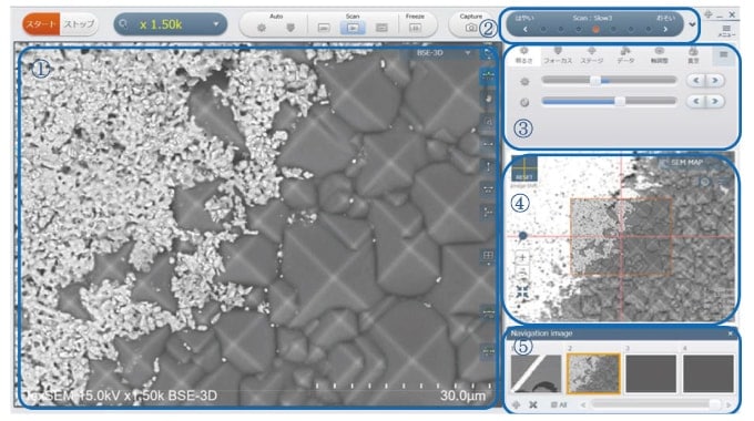
Fig 2. Screenshot of the FlexSEM GUI
A screenshot of the SEM MAP GUI is shown in Figure 3. The SEM MAP offers an intuitive approach to finding the field of view, which is a difficult task with conventional SEM instruments, and greatly reduces the difficulty of this task. In SEM observations, the specimen must be positioned inside a specimen chamber that is under vacuum, and thus cannot be directly viewed. In addition, because SEM images are black-and-white, it takes time to find the desired field of view—thus reducing throughput—when this is determined by information such as regions of discoloration, or when multiple specimens are mounted on the specimen stage. To solve this problem, a SEM MAP can display the interior of the specimen chamber to indicate the region of the specimen stage currently positioned for SEM image acquisition. Using this function, it is possible to create a map for navigation by attaching a previously captured external image (for example, by a digital camera or optical microscope image) or a SEM image that is acquired by pressing the Acquire Image Navigation Map button to the pattern diagram of the specimen stub. The created map simultaneously moves with the field of view due to movement of the sample stage. Therefore, specimen image which originally cannot see is capable of displaying as it can be seen directly.
The display corresponds to raster rotation of the image as well as stage movement, and the orientation of the SEM image display is aligned with the SEM MAP image all the time.
The map allows users to move rapidly to the desired position for observation by clicking the mouse on the map. In addition, the coordinates and the captured image position can be recorded and displayed on the SEM MAP.
An acquired SEM image can be layered on the camera navigation image. Also, different magnifications of an SEM image can be acquired. As shown in Figure 4, it is possible to switch to a high magnification image by scrolling the mouse wheel on the SEM MAP display. Thus, accurate navigation to an observation position is possible. In addition, the system is designed to allow intuitive operation other than the stage assist function, such as exchanging the detector signal by clicking each detector button or displaying the detector installation location, which is important information when X-ray analysis is performed.
Therefore, SEM MAP allows users to move rapidly and intuitively to the desired structures for observation, and can be expected to improve the throughput.
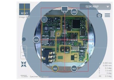
Fig 3. SEM MAP GUI screenshot
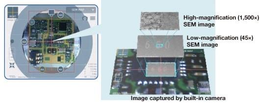
Fig 4. Enlarged image of SEM MAP
For the FlexSEM 1000, the axial autocalibration feature of the electron-optical system, which is installed in the high-end SU5000 model SEM system, has been enhanced with various automated alignment procedures, such as automatic alignment of the objective lens aperture and the optical axis, and astigmatism aberration corrections, which are performed after replacing a filament. Therefore, a high-resolution image without complicated manual axis adjustments is possible. Moreover, these automatic axis alignments also suppress shifting of the optical axis or the field of view that occurs when the electron beam current or accelerating voltage is changed. The time required for automatic brightness and focus adjustments has been decreased to approximately 2 seconds and 3 seconds, respectively, which is about 1/3 of the time required with the previous model. Thus, the total time for obtaining a focused image is reduced and a stress-free procedure for SEM observation is possible.
To improve the search process for the field of view in backscattered electron images, the FlexSEM 1000 is equipped with an image reconstruction filter to reduce the shifting of images in high-speed scans. Figure 5 shows images acquired before and after reconstruction. In the “before” image in Figure 5(a), the image is shifted and the desired field of view is very difficult to find without using a slow scan mode. The image reconstruction filter determines a deterioration function of the shifted image that is due to the detector system and preamp, and creates a reconstruction function by using an inverse convolution process. By applying the reconstruction function in real time to shifted images, shifting of images is reduced, as shown in Figure 5(b), and the field of view can be searched for in a fast scan mode in the backscattered electron image.
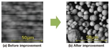
Fig 5. Backscattered electron images acquired with high-speed scan mode
Figure 6 shows example observations of impurities in resin using the SEM MAP function of FlexSEM 1000
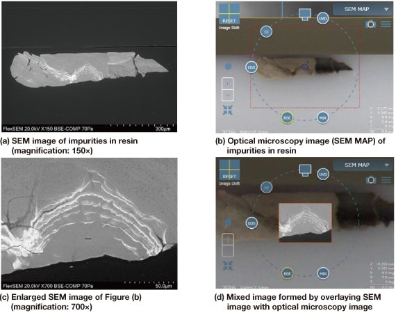
Fig 6. Examples of observation images using SEM MAP
Figure 6(a) shows an SEM image of impurities in resin, and Figure 6(b) shows a SEM MAP image that was captured using an optical microscope. The field of view for the SEM image corresponds to the rectangle in the optical micrograph. Even though the SEM image does not contain color information, the information can be obtained by observing the SEM MAP image. Also, information pertaining to impurities that are included in the surface or white resin can be obtained from the high-resolution image of SEM. Accurate observation positions can be obtained by using layered SEM images. Figure 6(c) is an enlarged SEM image of an impurity region and Figure 6(d) shows an SEM image layered with an optical microscopy image. In these images, a high-contrast striped structure can be observed in the impurity region. To identify the cause of the contamination, the impurity composition was investigated. Figure 7 shows elemental mapping images of impurities in the resin, which were acquired by using an X-ray analyzer. The specimen was milled by Hitachi High-Tech's IM4000 ion-milling machine and subjected to X-ray analysis under low-vacuum conditions without evaporation. Oxygen, titanium, and zinc were detected in the impurity regions. In the backscattered electron images, the high-contrast striped pattern corresponds to regions in which zinc has segregated. Titanium oxide and zinc oxide are both used as white pigments, and this pigment material can be assumed to have been mixed into the resin during the formation process.
An SEM image of zinc oxide is shown in Figure 8 as an example application. Because the FlexSEM 1000 uses a low-aberration lens to perform high-resolution observations, it is capable of observing the morphology of particles with sizes on the order of 50 nm at a high magnification of 50,000× at an accelerating voltage of 5 kV.
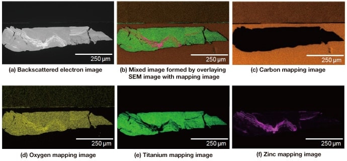
Fig 7. X-ray analysis images of impurities in resin
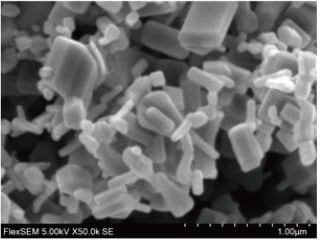
Fig 8. SEM image of zinc oxide
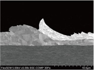
Fig 9. SEM image of Au bond
Figure 9 shows a cross-sectional image of an Au bond. The specimen was observed after preprocessing by an ion-milling machine. By using a high-sensitivity backscattered electron detector, a clear image of grain contrast in the material can be obtained. Figure 10 shows an image of hard candy. The surface of the candy is not heat-resistant and includes many needle-shaped crystals that are easily charged. However, a clear image of the specimen without charging or damaging it can be obtained by using the beam-brightness function, which ensures a stable emission current at low accelerating voltages and during integrated scanning.
Figure 11 shows SEM images of resin on a relay circuit board. The resin is non-conductive and observed under low-vacuum (50 Pa) conditions without metal coating evaporation. A backscattered electron image of the composition of the specimen is shown in Figure 11(a), and detailed topographical information for the specimen surface obtained using the Variable-Pressure Detector (UVD) is shown in Figure 11(b). Thus, different information can be obtained in the same field of view depending on the detector.
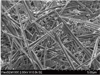
Fig 10. Image of hard candy

Fig 11. Images of resin on relay circuit board
In this report we have introduced the newly developed FlexSEM 1000, a compact, high-performance SEM that can be used for wide range of applications by novice to experienced users, and discussed the key features and function.
As examples of FlexSEM 1000 observations, we used application data for resins and metallic materials to demonstrate the high performance and simple operating functions. In the future, we are going to make an effort to provide leading-edge technology instruments that will support material development and analysis.
Publication data
Published in the monthly journal Engineering Materials (April issue 2017)
About the authors
* Hiroyuki Komuro
Science and Medical Systems Enterprise Unit
Scientific System Products Center
Electron Microscopy Solution System Design Group
Hitachi High-Tech Corporation
** Mari Sakaue
Science and Medical Systems Enterprise Unit
Scientific System Products Center
Applications Development Division
Hitachi High-Tech Corporation
See more
