Yo Yamamoto
Hybrid instruments that combine focused ion beam (FIB) methods with scanning electron microscopy (SEM) are valuable sample-fabrication tools that offer capabilities such as cross-sectional observation, transmission electron microscopy (TEM), and atom-scale probes of materials. They are used in a wide range of fields for structural analysis of materials such as metals, semiconductors, hybrid materials, and soft materials. In recent years, methods of 2D analysis—including observations of sample surfaces and analysis of local regions via TEM and other methods—have become insufficient for analyzing the structure of materials, which increasingly requires 3D analysis of mesoscale regions.
For this reason, there is a growing need for 3D structural analysis based on continuous cross-sectional observation methods using FIB-SEM. To address this, Hitachi High-Tech has developed high-performance FIB-SEM instruments and the Cut&See method for continuous cross-sectional observations.
This method continuously alternates FIB processing of evenly-spaced sample slices with in-situ SEM observations. The continuous SEM images thus obtained are then superposed on a computer at the intervals used for the FIB slicing step, yielding a 3D reconstruction of the structure. Moreover, because this method uses continuous cross-sectional SEM images, the spatial resolution of the 3D reconstruction is not affected by the thickness of the observed sample—an issue that is problematic for TEM analysis—offering the advantage of allowing high-resolution 3D analysis independent of sample thickness. In addition, this may be also utilized for the 3D elemental mapping or 3D crystal orientation mapping, by combined with analyzing method, such as energy-dispersive X-ray spectroscopy (EDS) or electron back-scattering diffraction (EBSD).
However, in general-purpose FIB-SEM systems, the FIB and SEM instruments are aligned at an angle to each other (this angle is 54° for Hitachi High-Tech instruments) to accommodate samples of various sizes., Therefore the direction of SEM observations is tilted with respect to the sample cross section. This can give rise to shifts in position during continuous cross-sectional processing, and differences in the horizontal-to-vertical aspect ratio of captured images, in which case the reconstructed structure does not necessarily match that of the original sample. In addition, the structure of FIB-SEM systems forces some unavoidable sacrifice of imaging performance compared to what is possible with a single SEM system, thus leaving some room for improvement. Also, the layout of conventional FIB and SEM systems ensures that the various detectors are not positioned optimally with respect to the sample, which places a variety of limitations on the system’s ability to capture in-situ continuous cross-sectional images (i.e.. real-time 3D analysis).
At Hitachi High-Tech we have transcended these traditional approaches to FIB-SEM system design by developing the NX9000 FIB-SEM Real-Time 3D Analyzer, an instrument boasting an orthogonal layout in which the FIB and SEM systems are aligned at a 90° angle to each other, and the positions of the lens barrel, the sample stage, the detectors, and other elements are optimized to solve all of the problems mentioned above.
In this report, we discuss the key features of the NX9000 for 3D analysis and present sample applications involving analysis of semiconductor devices and batteries.
Figures 1 and 2 show a photograph of the NX9000 and a schematic diagram of its internal structure, respectively.
The instrument is equipped with a newly developed cold-cathode field-emission scanning electron microscopy (cold FE-SEM) lens barrel. In addition, to fully extract the SEM performance in observing FIB-processed cross sections, the FIB lens barrel is aligned perpendicular to the SEM at an optimized working distance (WD) of 4 mm. This improves the image resolution of SEM observations at the beam crossing point (CP) compared to tilted FIB-SEM systems, and also allows real-time SEM observations via vertical irradiation of the sample cross section. This eliminates the artifacts of conventional tilted FIB-SEM noted above—position shifts during continuous cross-sectional processing and horizontal-to-vertical aspect-ratio variations due to the tilted observation—allowing faithful reconstruction of the 3D structure of the sample.
In addition, the instrument includes a miniature sample stage equipped with a high-precision scale, allowing a significant reduction in system drift. This allows high-stability, high-precision continuous FIB cross-sectional processing with continuous SEM cross-sectional observations, enabling high-quality 3D structure observation using the Cut&See method. Also, miniaturizing the sample holder allows the system to enter a low-drift state immediately after sample placement, improving throughput for 3D observations.
Finally, by optimizing the relative positions of the sample, lens barrels and the various detectors—including the SEM electron detector and the EDS and EBSD detectors—we have made it possible to obtain signals from various detector systems at the CP, allowing not only the structure of the sample but also 3D information on properties such as material composition and crystal structure to be gathered simultaneously.
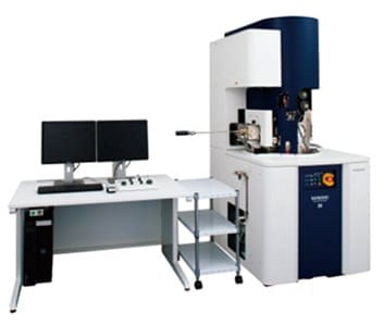
Fig.1 The NX9000
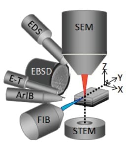
Fig.2 Schematic diagram of the internal structure of the instrument
In what follows we present the key features and functionality of the NX9000.
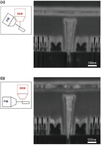
Fig.3 Cross-sectional SEM images of a flash-memory sample
(a)Image observed with a conventional tilted system
(b)Image observed via vertical irradiation using the NX9000
FIB-processed sample cross sections may be observed in-situ via SEM images captured vertically, offering even higher resolution and contrast. In addition, vertical irradiation by the electron beam improves the horizontal-to-vertical aspect ratio of the resulting images, allowing information on the dimensions of samples to be obtained with greater accuracy than with conventional approaches.
Using a commercial 2X NAND flash-memory sample, we compared SEM cross-sectional images captured by the NX9000 and by a conventional tilted FIB-SEM system. The results are shown in Figure 3. Figures 3(a) and 3(b) are secondary-electron images obtained at the location of the CP under identical beam conditions using the conventional system and the NX9000, respectively. Because the orthogonal alignment of the lens barrel allows the internal design of the NX9000 to be optimally arranged, cross-sectional images observed in-situ exhibit accurate horizontal-to-vertical aspect ratios and improved resolution and contrast compared to those obtained by conventional methods.
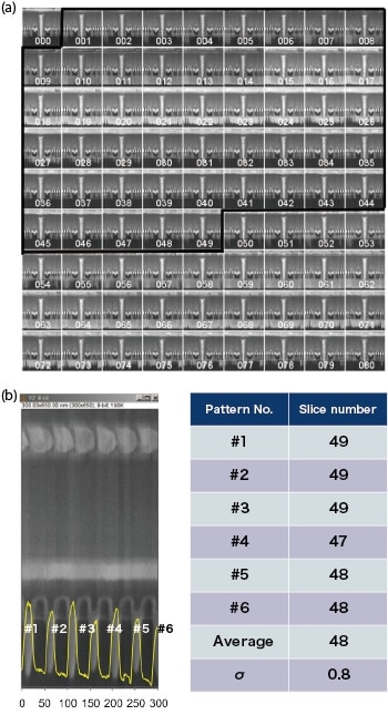
Fig.4 Reproducibility of slice processing
(a)Continuous cross-sectional SEM images
(b)Reconstructed image of YZ cross section and number of processed slices for the repeating patterns
In addition to the high-performance sample processing made possible by the FIB lens barrel, the inclusion of a low-drift miniature sample stage allows the NX9000 to achieve highly reproducible slice processing. This enables Cut&See automated continuous operation with intervals on the order of nanometers for long periods of time in a stable state.
Figure 4 shows the results of tests to verify the reproducibility of slice processing using a commercial 2X NAND flash-memory sample.
We set the step size for continuous slice processing to 1 nm and considered 6 processing patterns involving repeated STI/Si steps, simultaneously observing SEM images. We used the continuous SEM images thus obtained to reconstruct an image of the YZ cross section and measured the number of processing slices produced by the repeated pattern.
The results indicate an average of 48 slices per pitch with fluctuations (σ) of 1 slice or less. This demonstrates the extremely high precision and reproducibility of the continuous slice processing capability of the NX9000.
The standard NX9000 comes equipped with one secondary-electron detector in the sample chamber (lower SED), In-column secondary-electron detector (upper SED), and In-column backscattered-electron detector (BSD), and images can be captured by these detectors simultaneously.
Figure 5 shows an example in which the surface of a lithium-ion battery material was observed by the various detectors.
Images captured by the lower SED, the upper SED, and the BSD are shown in Figures 5(a), 5(b), and 5(c), respectively. Each image exhibits characteristic features: the lower-SED image highlights surface roughness, the upper-SED image highlights the state of the surface—including the fine-grained surface structure and the electrostatic potential—and the BSD image highlights the material composition. The simultaneous capture of all three images demonstrates the ability of the NX9000 to obtain multiple types of information—including surface morphology, fine-grained structure, and material composition—simultaneously.
In 3D FIB-SEM observations, cross-sectional FIB processing and cross-sectional SEM observations are performed continuously; because these are destructive processes, it is important to obtain multiple types of information simultaneously during the measurement. Figure 6 shows examples of 3D observations of a fuel-cell electrode material as captured using the simultaneous three-detector capture capabilities of the NX9000. This sample has a three-phase structure consisting of YSZ, Ni, and voids (filled with resin). For structural analysis, these three phases must be separated and analyzed. This would be difficult to do using images from just a single detector, but here it is readily accomplished thanks to the ability of the NX9000 to capture images from three detectors simultaneously. Thus, by exploiting simultaneous image capture from three detectors each offering distinct features, all available information is captured from the sample and an accurate 3D structure is obtained.
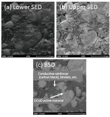
Fig.5 Imaging the surface of a lithium-ion battery material
(a) Lower SED image
(b) Upper SED image
(c) BSD image
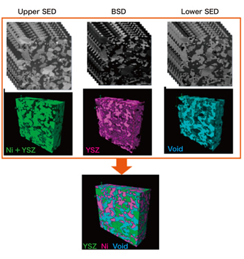
Fig.6 Example of a 3D observation of fuel-cell electrode material using simultaneous image capture by multiple detectors
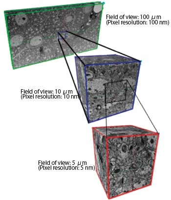
Fig.7 High-resolution, wide field-of-view image of mouse brain cell tissue obtained using Multi-Cut & See
In materials analysis, acquiring knowledge about the fine-grained structure of a material requires high-resolution observations. High-resolution observations are achieved by using high magnification factors in SEM observations; however, this reduces the area of the observed region. For materials or biological samples that exhibit random structures, not only high-resolution observations of localized regions are required, but also observations over wide sample areas, in order to elucidate the relationship between these regions and their surroundings.
However, high-resolution observations over wide fields of view require large image-acquisition times and produce large volumes of data. For example, if we wish to obtain an image with a field of view of 100 × 100 µm and a resolution of 5 nm, the number of data points acquired—that is, the number of pixels in the image—is 20,000 × 20,000, and the measurement will require enormous amounts of time and data storage capacity. To alleviate this difficulty, Hitachi High-Tech has developed Multi-Cut&See as a tool for high-resolution 3D analysis with wide fields of view. With this capability, the position and spatial extent of the image acquired for each cross-sectional surface during continuous cross-sectional observations may be chosen arbitrarily, and multiple images may be acquired. This allows not only acquisition of high-resolution images of a sample region at high magnification, but also wide field-of-view observations of the surrounding region at low magnification.
Figure 7 shows an example in which Multi-Cut&See was used to observe mouse brain cell tissue. In this example, the number of pixels per image is 1,000 × 1,000, and images were acquired with fields of view of 5, 10, and 100 µm. This allows acquisition of continuous images at a high resolution of 5nm and continuous images spanning a wide area of 100 µm in the same region. In this case, the total number of pixels is 1,000 × 1,000 × 3. Compared to acquiring an image with a 100 µm field of view at 5 nm resolution, this method reduces both time and data volume by more than a factor of 100, yielding an extremely efficient data-acquisition technique.
In combination with Cut&See, continuous EDS elemental mapping (3D-EDS) and continuous EBSD crystal-orientation mapping (3D-EBSD) data may be acquired automatically with no need to move the sample stage. This allows stable acquisition of 3D structural, composition, and crystal-orientation data, leading to a system for producing a thorough portfolio of 3D data for materials analysis.
Figure 8 shows an example of a 3D-EDS analysis involving a fuel-cell electrode material (Ni-YSZ). EDS mapping allows accurate separation of elements in the various phases within the sample interior (Zr, O, Ni, and voids), enabling analysis of their 3D distribution.
Figure 9 shows an example of a 3D-EBSD analysis involving a Ni-based metallic material. By optimizing the alignment of EBSD, FIB, and SEM, there is no need to move the sample stage between the continuous cross-sectional processing and measurement phases, allowing acquisition of stable, continuous maps of crystal orientation.
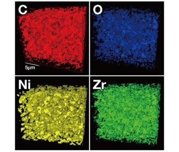
Fig.8 Example of a 3D-EDS analysis
Sample: Fuel-cell electrode material (Ni-YSZ)
Mapping acquisition interval: 100 nm
Number of mappings: 212
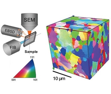
Fig.9 Example of a 3D-EBSD analysis
Sample: Ni
SEM accelerating voltage: 20 kV
Mapping acquisition interval: 150 nm
Number of mappings: 150
In this report we have presented the key features and functions of the Real-Time 3D Analytical FIB-SEM 'NX9000', a new instrument developed by Hitachi High-Tech to meet the growing need for FIB-SEM-enabled analysis systems for collecting 3D information on mesoscale material regions.
Through a series of practical case studies, we demonstrated that the NX9000—paired with our Cut&See package—is an extremely powerful tool for 3D structural analysis of materials, and is expected to be widely adopted for various fields.
Acknowledgements
Fuel-cell electrode samples (Ni-YSZ) were provided by Professor Naoki Shikazono of the Institute of Industrial Science, the University of Tokyo. Mouse nerve-tissue samples were provided by Associate Professor Yoshiyuki Kubota of the Division of Cerebral Circuitry, National Institute for Physiological Sciences. To both we extent our deepest gratitude.
Publication data
Published in the monthly journal Engineering Materials (September issue 2017)
Authors
Yo Yamamoto
Beam Technology Systems Design Department
Hitachi High-Tech Science Corporation
See more
