Masataka Ohgaki
The electroless Ni-P/Au plating that have become available in recent years have played a crucial role in the deleading efforts of the late 1990s, but they have been reported to exhibit relatively unreliable solder-ball connection reliability compared to other surface treatments, among other issues1-4). The electroless Ni/Pd/Au plating that have been considered as potential substitutes clearly exhibit a level of solder-ball connection reliability comparable with that of electrolytic Ni/Au plating or preflux, and they have become increasingly general-purpose products. With regard to the connection damage of electroless Ni-P/Au plating, research has confirmed that many of the regions that suffer damage lie at interfaces between the solder and electroless Ni-P plating, with microscopic surface cracks forming at grain boundaries at the plating-layer interface; in contrast, in electroless Ni/Pd/Au plating the Ni layer interface is shielded from corrosion by the Pd layer and is thus of high quality.
Since the 2000s, the establishment of RoHS directives regarding toxic substances has forced many producers of electronic components to carry out a major overhaul of their manufacturing processes and to diversify the combinations of mounted components, substrates, and surface-mount processes they use. This development has made Ni/Pd/Au plating a focus of intense interest, and the pursuit of techniques for producing plating products of ever higher quality has spurred a variety of studies to assess factors such as variations in film thickness and film adhesion, and the fatigue performance.
As plating evolve into increasingly multilayered structures, the reliability of the various junctions that form at layer interfaces has emerged as a key quality metric affecting the performance of components themselves, and the effectiveness of methods for analyzing plating has become a key point of concern in the design of the plating layers that form the component base for product development and technology rollout. In this report, we present our recent success in adapting a method for film-thickness measurement via energy-dispersive fluorescent X-ray spectroscopy to the analysis of plating.
The renewed need to conduct not only surveys of the state of plating surfaces and layer-interfaces, but also reliability tests and failure analyses for components, highlights the importance of various environmental tests and non-destructive methods of examination and analysis. Among these approaches, methods of non-destructive analysis using X-rays have been applied in a particularly wide variety of settings.
Table 1 lists methods commonly used to analyze the thickness of plating. Methods based on fluorescent X-rays use standard samples to achieve non-destructive, non-contact measurements that can characterize the plating thickness of ultra-miniature components in short periods of time. For alloy plating, these methods can not only measure the film thickness of alloy plating, but can also determine the alloy composition and perform simple elemental analysis, with additional operations such as automated measurement and statistical processing also available.
Fluorescent X-ray analysis is used primarily to analyze the elemental composition of substances and measure the elemental distribution on surfaces; it is an effective tool for measuring film thickness in multilayered coatings and identifying the elements and impurities present in plating layers. Moreover, by extracting cross-sectional slices from the plating layers one can measure the elemental distribution (i.e., perform elemental mapping). Not only do electroless Ni-P plating contain P levels up to several tens of wt%, but the plating bath used at the processing stage may also contain trace quantities of Pb or S added as stabilizers to suppress reactions and self-decomposition4,5).
Methods for using fluorescent X-ray analysis to make quantitative measurements may be divided into two categories: calibration-curve methods and fundamental-parameter (FP) methods. In the former approach, a reference substance is used to construct calibration curves from the relationship between concentration and X-ray intensity for known sample components, and this is used to compute the concentration of unknown components of a sample. In contrast, FP methods are based on theoretical computational techniques and have the advantage of yielding quantitative results easily, with no need for reference substances when measuring unknown components. In recent years, the convenience of the FR approach has made it an increasingly mainstream option.
Assuming a number of conditions are satisfied—that the sample is uniform, sufficiently large and thick, and that the total quantitative value for all elements is 100%—the overall agreement in the computational simulation process between the measured element concentration and the computed estimate of the concentration will be accurate, allowing rapid and precise quantitative analysis. In addition, for thin-film samples, by inputting structural data on the film one can exploit the correlation between film thickness and X-ray intensity from structural elements in the film to measure film thickness in a non-destructive way. Both calibration-curve methods and FP methods may be used to measure the film thickness, but calibration-curve methods for multilayered films require multiple standard substances, so for this case the use of FP methods—which yield measurements with no standard samples—is particularly valuable.
At Hitachi High-Tech Science, we have commercialized two series of instruments for fluorescent X-ray analysis: the EA series of instruments, primarily for elemental analysis, and the FT series, primarily for film-thickness measurements. Figure 1 shows our latest plating thickness gauge, the FT150. In this report we present practical examples of thin-film measurements for plating using fluorescent X-rays.
| Description | Features | |
|---|---|---|
| Microscope cross-sectional observation methods |
A cross section of the sample is sliced, embedded in resin, polished, and etched, and a vertical cross section of the plating is observed using a microscope to determine the coating thickness. The image may be recorded and stored, making this a basic method for thickness measurements. However, it is cumbersome and requires experience, and does not allow easy measurement of films that are less than 1-µm thick. | Allows thickness measurements for samples with thicknesses up to several tens of micrometers, including microscopic regions and complicated sites. Also useful for observing the presence, absence and structure of plating layers and for identifying the causes of plating failures. |
| Electrolysis methods |
A microscopic region of a plating is anodically dissolved and removed at a fixed electrolysis current. Measurements of coating thickness are based on the fact that the time required for this process is proportional to the plating thickness. | Can measure thicknesses of many types of plating, and can determine individual film thicknesses for multilayered plating. Cannot measure small items or sites with complex shapes. |
| Magnetic force methods |
To determine the plating thickness, these methods measure the variation in magnetic attraction between a magnet and a base metal, or the magnetic resistance of the magnetic flux through the plating and base metal, arising due to the difference in thickness of a non-magnetic plating on a magnetic base metal. | May be used to measure the thickness of non-magnetic plating films on ferromagnetic materials. Thus it is applicable to plating such as zinc, copper, chrome, and tin on iron. |
| Fluorescent X-ray methods |
A fluorescent X-ray thickness analyzer irradiates a plating sample with X-rays, and the fluorescent X-rays emitted by the plating are measured to determine the plating thickness. Due to the basic mechanism of this measurement, it suffers large errors in cases where the plating metal and the base material have similar atomic numbers. Also, the measured value corresponds to the thickness of a pure metal plating film, so the density (purity) of the film affects the plating thickness result. | If a standard sample is used to produce a calibration curve in advance, this method can make non-destructive, non-contact measurements of the plating thickness of microscopic components in short periods of time. For alloy plating, this method measures the plating film thickness and alloy composition, performs simple elemental analysis, and offers automated measurements and statistical processing functionality. |
| β-ray methods | These methods use a β-ray thickness analyzer to irradiate a sample with β-rays and measures the backscattered β-rays to determine the plating thickness. | The basic method is similar to fluorescent X-ray methods. By way of comparison, β-ray methods cannot be used to make non-contact measurements, but can measure thick coatings, hard plating, various types of waxes, and paint films on plastics. |
| Multiple interference methods |
A portion of a sample coating is removed by dissolution, or a portion is masked before plating, to create a gap. Then a multiple-interference thickness analyzer is used to irradiate the sample and a reference slab with monochromatic light and the plating thickness is determined from the shift of the interference fringes. | Requires a Fizeau multiple-interference thickness analyzer. |
| Eddy current methods |
A high-frequency current is passed through a probe (measurement terminal) to induce eddy currents in surface regions of the plating under investigation; the variation in eddy current with electrical conductivity, thickness, and shape is measured and used to determine the plating thickness. | The plating and base materials must have sufficiently different electrical conductivity; the method is used for zinc plating on steel plates or copper plating on printed circuit boards. |
| Micrometer methods |
These are methods in which a micrometer, dial gauge, surface roughness analyzer, or similar instrument is used to measure the thickness of a plating on a metallic or non-metallic base material. The method may be destructive to the plating, destructive to the base, non-destructive, or contact-based, with the appropriate method chosen based on the nature of the plating. | Used in cases where typical plating-thickness gauges cannot be used, or to measure extremely thin films such as evaporated films. |
| Plating adhesion quantity testing via mass analyzers |
These are methods in which the quantity of a plating adhering to a metallic or non-metallic base material is measured by a mass analyzer. The method may be a mass measurement that is destructive to the plating, an analytical method that is destructive to the plating, a method that is destructive to the base, or a non-destructive method, with the appropriate method chosen based on the nature of the plating. | Applicable to cases where it is necessary to measure the plating adhesion for an entire sample from the partial thicknesses of the plating. May be used to measure thick precious metal plating, compound plating, alloy plating, and other similar plating. |
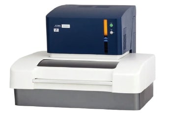
Fig. 1 The FT150 Fluorescent X-ray coating thickness gauge
Chip components, typified by laminated ceramic-chip capacitors, are among the most important components in smartphones and on-board computers. In recent years, the miniaturization and increasing sophistication of products has driven advances in high-density surface-mounted installation, with the components themselves becoming extremely small. Many such ceramic-chip capacitors use a bilayer Sn/Ni film in electrode regions, and these films require quality control of thickness. However, for thick Sn layers the fluorescent X-rays emitted by Ni are strongly absorbed by the Sn, complicating the simultaneous measurement of Sn and Ni. Here we illustrate film-thickness measurement for multilayered films by performing a simultaneous measurement of an Sn/Ni bilayer on Ag, designed to resemble a ceramic-chip capacitor.
The simulated-capacitor samples we study are prepared using Ag, Ni, and Sn thin-film standard substances from Hitachi High-Tech Science; we first form an Ni layer on Ag, then add an Sn layer to yield an Ag/Ni/Sn multilayered film. We prepared samples with three different layer-thickness combinations, as follows:
Sample A: Ag 2.01 µm / Ni 1.90 µm / Sn 8.95 µm
Sample B: Ag 4.61 µm / Ni 1.90 µm / Sn 8.95 µm
Sample C: Ag 9.43 µm / Ni 4.89 µm / Sn 8.95 µm
For this analysis, we registered one reference substance consisting of 8.95 µm Ag, 4.89 µm Ni, and 4.61 µm Sn on an Al substrate (all metals were thin-film standard substances from Hitachi High-Tech Science). Our measurement used the Kα lines of Sn, Ni, and Ag as analysis lines and employed a tube voltage of 45 kV, a beam diameter of 35 µm (where the beam diameter is defined as the diameter containing 90% of the intensity of primary X-rays with energies in the range 30-40 keV), a primary filter of an Al plate, and a measurement time of 30 s, using a thin-film FP method.
For samples A, B, and C, we made 10 measurements each of Sn and Ni in a microscopic region. Table 2 shows the accuracy of our thickness measurements and the results of an assessment of their repeatability.
| Sn layer | Ni layer | Ag layer | ||
|---|---|---|---|---|
| Sample A | Mean value (µm) | 2.01 | 1.94 | 8.89 |
| Standard deviation | 0.051 | 0.037 | 0.046 | |
| RSD% | 2.5% | 1.9% | 0.5% | |
| Sample B | Mean value (µm) | 4.63 | 1.93 | 8.82 |
| Standard deviation | 0.049 | 0.043 | 0.050 | |
| RSD% | 1.1% | 2.2% | 0.6% | |
| Sample C | Mean value (µm) | 9.36 | 4.65 | 8.84 |
| Standard deviation | 0.068 | 0.164 | 0.122 | |
| RSD% | 0.7% | 3.5% | 1.4% | |
For the three samples with differing thickness of Sn and Ni, the measurements indicated a repeatability of better than 96%, which is an excellent result despite the measurement time of 30 s. In addition, we obtained highly accurate measurements of the thickness of Ni films below a thick (approximately 10 µm) Sn film. This demonstrates the possibility of accurate simultaneous measurement of Sn/Ni bilayers.
Thus, by using mock samples it is possible to check the accuracy and efficacy of film-thickness measurements of actual target samples.
Figure 2 shows a comparison of fluorescent X-ray spectra for an Sn sample with a thickness of approximately 5 µm obtained using Hitachi's previous-generation instrument and using its latest instrument. The latest instrument uses a new light-focusing optical system and a high-sensitivity detector to yield a significant improvement in sensitivity to the Sn Kα line, which has previously been difficult to measure, and the remarkable progress in energy-dispersive fluorescent X-ray analyzers is plain to see.
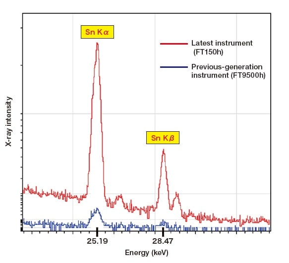
Fig. 2 Comparison of spectra measured for a 5 µm-thick Sn sample.
Items of interest when performing plating surface observations include the nature of the surface, its physical properties, impurities, corrosion, and the state of whisker formation. For Ni/Au plating, the presence of pinholes in the Au layer can promote corrosion in the underlying Ni layer and advance the hole, significantly degrading the reliability of the plating. In contrast, in Ni/Pd/Au plating the Pd layer serves to prevent this; moreover, the adhesion at the interface is adequately secured, yielding dramatic improvements in reliability. However, in cases involving an extremely thin Au layer, one cannot neglect the possibility that any extremely non-uniform regions that may be present might serve as the origin of problems, and thus it is important to make effective use of plating surface observation.
For our electroless Ni/Pd/Au plating formed on Cu, we prepared a 20 mm × 20 mm thin plate consisting of an array of coating patterns with a diameter of 300 µm. We attached a Cu foil to a base material surface with a glass epoxy resin laminated by an interlayer insulating material and constructed a multilayered plating film as follows.
First, we applied a Pd catalyzation treatment to the Cu surface of the base material, and then applied an electroless Ni coating treatment (P content: 6-7 wt%) to form a layer. On this we applied an electroless Pd coating treatment (P content: approximately 4 wt%), and then a substitute Au coating treatment to the outermost layer to fabricate a multilayer plating. Thus, the electroless Ni/Pd/Au multilayered coating used in our experiments is accurately described as an electroless Ni-P (P: 6-7 wt%) / Pd-P (P: 4 wt%) / Au multilayered coating on Cu. For electroless plating fabricated in this way, it is commonly known that the Ni coating layer forms an amorphous eutectic with P, while the Pd layer forms a low-crystallinity eutectic with trace amounts of P.
Figure 3 shows tilted and non-tilted SEM images (secondary electron images) of the surface of the electroless Ni/Pd/Au plating on Cu, together with higher-magnification images. In the low-magnification images, in which the outer perimeter of the array pattern is discernible, it can be seen that the plating is generally uniform, although there is some surface roughness [Figure 3 (a, c)]. In the high-magnification images, grains and grain boundaries are clearly visible at the coating surface layer, and the surface is formed by a densely packed layer of structural grains of roughly uniform size [Figure 3 (d)]. The tilted image in Figure 3 (b) shows that the surface roughness is not particularly significant [Figure 3 (b)].
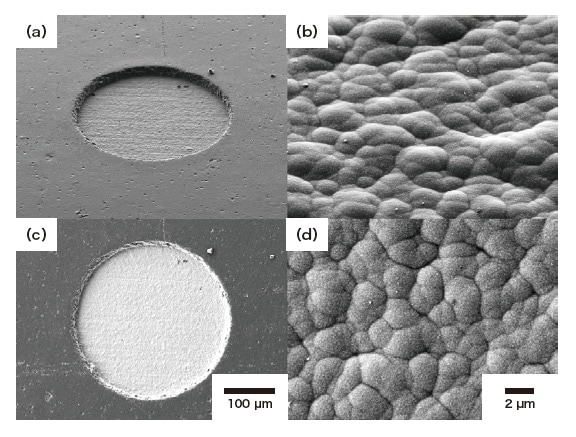
Fig. 3 SEM (secondary electron) micrographs of Ni/Pd/Au plating surface on Cu.
In fluorescent X-ray coating thickness gauge that irradiate the sample in the vertical direction from above, the primary X-ray beam emitted from the X-ray tube is constricted by a capillary and passes through a sample observation mirror before impinging on the sample. For the data measurements we present here, we used an instrument whose optical system is capable of tightly focusing the beam using a capillary.
In the atoms comprising the sample, electrons are excited by the primary X-rays and emit fluorescent X-rays. These are counted by a detector, and the sample thickness and composition are computed from the X-ray intensity thus obtained. The accuracy of film-thickness measurements made in this way depends to a significant extent on statistical fluctuations in the counted X-ray intensity. Thus, in addition to maximizing the X-ray count by using a high-intensity primary X-ray beam and choosing appropriate settings for the measurement time and other conditions, we take the mean value of repeated measurements and estimate errors from the standard deviation and other factors.
Also, although for film thickness determined with fluorescent X-rays it is desirable to use calibration curves for standard substances and reference values for samples of known thicknesses, nonetheless the results are affected by factors such as film purity and differences in the densities of films. For this analysis we use a standard substance consisting of an electroless Ni/Pd/Au multilayered plating of known thickness on a Cu substrate (infinite-thickness Cu / 5.09 µm Ni / 0.048 µm Pd / 0.051 µm Au) and use the following measurement conditions: primary X-ray excitation voltage 30 kV, beam diameter 0.1 mm, measurement time 60 s, and an ambient environment.
Table 3 lists the thicknesses of the various layers determined by fluorescent X-ray coating thickness gauge measurements for one element in the array of patterns of electroless Ni/Pd/Au plating on Cu. The table lists the mean value of 10 repeat measurements, as well as the standard deviation (σ) and relative standard deviation [CV (%)]. The results indicate that the mean measured thicknesses of the various layers are sufficiently large compared to their standard deviations to be significant, and we find thicknesses of approximately 50 nm for the Au layer, approximately 80 nm for the Pd layer, approximately 3.1 µm for the Ni layer, and approximately 6.3 µm for the Cu layer. The standard deviation of the thickness of the Cu layer—the lowest base-material layer—is slightly larger than that for the other layers. We attribute inaccuracies in the measured thickness of the Cu layer to significant surface roughness at the interface with the underlying base layer—visible in cross-sectional SEM observations, as discussed below—which complicates measurements of film thickness.
| Au layer | Pd layer | Ni layer | Cu layer | |
|---|---|---|---|---|
| Mean value (µm) | 0.049 | 0.082 | 3.081 | 6.308 |
| Standard deviation | 0.001 | 0.002 | 0.012 | 0.033 |
| RSD% | 1.88% | 1.85% | 0.40% | 0.52% |
(1) Film thickness measurement via cross-sectional observation and length measurement
We used a hybrid FIB-SEM (focused ion beam - scanning electron microscope) instrument to prepare a cross-sectional plating surface and measured the thicknesses of the plating layers. Processed sample surfaces prepared by FIB may be observed without additional processing or modification, using SEM from a tilted direction. Tilt correction can be applied to convert tilted images to frontally-observed images.
Figure 4 shows images obtained by in-situ SEM observation of FIB-prepared cross-sectional plating surfaces. The state of each layer is observed clearly with high contrast. There is some fluctuation in the thickness of the layers, but the interface adhesion is high, and the locations of the interfaces can be clearly identified. Cross-sectional SEM observation also yields information on the structure of each layer; for example, in the Cu, Pd, and Au layers the contrast due to crystal grains is clear, and for the Cu layer in particular we see that relatively large crystal grains with different orientations form the layer. Small crystal grains are also observed in the Pd and Au layers, so these layers have a certain amount of crystallinity. However, for the Ni layer there is no clear indication of crystal grains or grain boundaries, suggesting a high likelihood that this layer has a low degree of crystallinity.
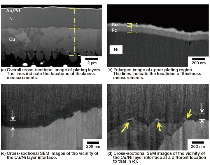
Fig. 4 Cross-sectional SEM images of Ni/Pd/Au plating on Cu, prepared via FIB
Table 4 compares the mean values of 10 thickness measurements for each coating layer using cross-sectional SEM images to film thicknesses measured using a fluorescent X-ray coating thickness gauge. The two sets of measurements are in reasonable agreement; however, whereas the two measurements yield nearly identical values for the thickness of the uppermost Au layer, there is some disagreement for the thicknesses of inner layers. One possible reason for the imperfect agreement is that, for thickness measurements via the fluorescent X-ray coating thickness gauge, the densities of the substances in the actual layers may differ from those of the standard sample used as a reference and there may be difference in quality (including factors such as fine-grained structure and purity) between layers. For this analysis we have assumed that the Pd and Ni layers are composed of single-phase Pd and Ni when calculating film thicknesses, whereas in fact the layers contain small quantities of P (that is, they are Pd-P and Ni-P mixtures), and we attribute the disagreement in film thickness to this fact.
Also, as discussed above, there is significant surface roughness at the interface between the Cu and the base material, yielding significant differences in thickness depending on the measurement location. In cases like this, in which film thicknesses differ depending on measurement conditions, one must carefully consider the use of the method by taking into account the impact of site-dependent thickness measurements and the significance of adopting a mean thickness value. In addition, the fluorescent X-ray film-thickness results may exhibit small variations depending on the choice of computation method.
| Au (µm) | Pd (µm) | Ni (µm) | Cu (µm) | |
|---|---|---|---|---|
| Measurement of fluorescent X-ray coating thickness gauge* | 0.049 | 0.082 | 3.08 | 6.31 |
| Measurement from FIB-SEM cross section** | 0.047 | 0.094 | 3.48 | 6.31 |
With proper handling of the various factors discussed above, the measured data approach the true film thicknesses. In practice, a recomputation for the same sample using the same fluorescent X-ray data but with the compositions of the Ni and Pd layers changed to Ni-P (7 wt%) and Pd-P (4 wt%) produced thickness values of 0.049 µm for the Au layer, 0.102 µm for the Pd-P layer, 4.10 µm for the Ni-P layer, and 6.68 µm for the Cu layer. The Pd-P layer thickness obtained in this way is close to the FIB-SEM value of 0.094 µm for the Pd-layer cross section. In this case, the different measurement methods yield different values for the Ni layer thickness; factors contributing to this discrepancy include the large surface roughness at the interface with the underlying Cu layer and the fact that the Ni layer is amorphous, whereupon no precise value for its density may be established.
Therefore, we investigated the internal structure of each layer in greater detail. In electroless Ni/Pd/Au plating it is believed to be rare for alloys to form between layers8); however, cross-sectional SEM images of the coating layer [Figure 4 (a)] indicate, at the Cu-Ni interface, a relatively dark layer that differs from the layers above and below it. In addition, at the Ni-Pd interface there are occasional voids. In the SEM image in Figure 4 (b), there are also voids on the Ni side of the Ni-Pd interface (near the right edge of the image). These are instances in which Ni grain growth within the Ni layer proceeded from both sides and the grains became attached, making them more susceptible than other regions to the accumulation of corrosion. In plating consisting of Ni layers alone, these voids grow downward and form pinholes and cracks, inviting corrosion of the Cu layer; however, in electroless Ni/Pd/Au plating, the overlying Pd/Au layers prevent the diffusion of voids, as shown in this image, serving to protect against the advance of corrosion and deterioration to some extent.
Figure 5 (a) shows an overall STEM image of a cross-sectional plating sample prepared via FIB processing of a coating sample fabricated by the same process used to fabricate the sample discussed above. In the Cu layer underlying the sample, crystal grains with contrast variations arising from differences in crystal orientation are clearly visible; meanwhile, the interfacial layer between the Cu and Ni layers, discussed above, exhibits image contrast similar to that of the Ni layer, as in the SEM image. Also, in the Ni layer, voids can be seen near the Pd interface. The thin striped lines in the horizontal direction visible in Figure 5 (c) are thought to be associated with the formation of coating layers; however, although grains with sizes of 3-4 nm are observed in the Ni layer, none of these are clear, indicating an amorphous structure.
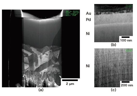
Fig. 5 STEM image (accelerating voltage: 30 kV) of cross-sectional thin sample of Ni/Pd/Au plating on Cu
(2) Fine-grained observation of coating interfacial layers
Here we observe the interior structure of the plating in an effort to clarify fine details. Figures 6 (a) and 6 (b) respectively show STEM images of the vicinity of the Cu-Ni interface and a cross-sectional STEM image including portions of the Ni, Pd, and Au layers. In these STEM images, crystal grain boundaries in the Cu layer are visible even more clearly than in the SEM images, and differences in the crystal orientations of grains are also clearly shown. The brightness of the intermediate layer along the Cu-Ni interface is almost the same as that of the Ni layer, and there is no alloy formation accompanied by prominent crystal growth. The results of an analysis of all layer interfaces to detect the presence of intermediate layers revealed that an interfacial layer is present between the Cu and Ni layers, but no clear interfacial layer is observed at the Ni-Pd or Pd-Au interfaces.
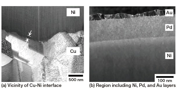
Fig. 6 STEM images (accelerating voltage: 30 kV) of Ni/Pd/Au plating layer on Cu
Clear information on the vicinity of these interfaces may be obtained by capturing TEM images. Figure 7 shows high-resolution TEM images of the Au-Pd and Pd-Ni interfacial regions. In the Au-Pd interface image [Figure 7 (a)], the lattice fringes in the highly crystalline Au layer exhibit a slight distortion in the vicinity of the interface with the Pd layer, and are tightly coupled with the lattice in the Pd layer. In the coupling region there is some distortion of the lattice structure of the two crystal phases and some degradation in crystallinity due to lattice mismatch, but no change in the lattice spacing and no evidence of an alloy layer. At the Pd-Ni interfacial region, there is a low-crystallinity Pd crystallite with distorted lattice fringes, coupled to a Ni crystallite of yet lower crystallinity (almost amorphous), and a shared region of lattice mismatch. Again at this interface no alloy layer or other interfacial layer is observed.
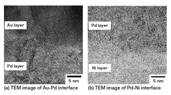
Fig. 7 High-resolution TEM images of interfacial regions in Ni/Pd/Au plating
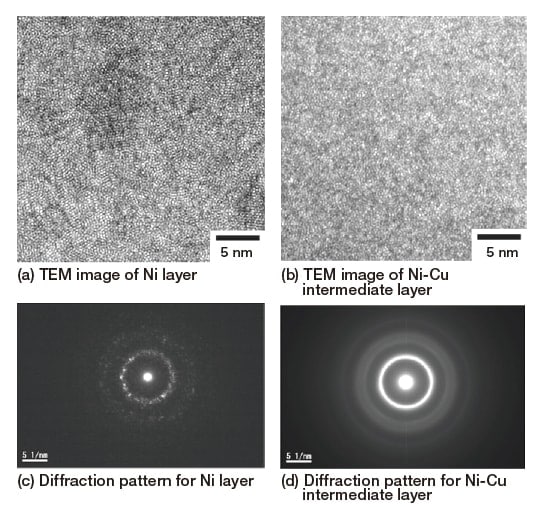
Fig. 8 High-resolution TEM images and electron-beam diffraction patterns for Ni layer and Ni-Cu intermediate layer in Ni/Pd/Au plating
The interfacial layer between the Cu and Ni layers is observed as a region of different brightness from the central region of the Ni coating layer. To clarify the difference between this interfacial layer and the Ni coating layer, Figure 8 shows high-resolution TEM images and electron-beam diffraction patterns for both. In the TEM image of the Ni coating layer [Figure 8 (a)], small crystallites in which the crystal lattice is preserved are visible at scattered sites within the overall low-crystallinity—nearly amorphous—structure. In contrast, in the TEM image of the Cu-Ni interfacial layer there are extremely few crystallites in which lattice fringes can be recognized. Also, the diffraction pattern for the interfacial layer [Figure 8 (d)] is ring-like with no evidence of spots, again indicating that this region is completely amorphous. Thus, although the Ni layer in electroless Ni/Pd/Au multilayered coatings is commonly said to be amorphous, in fact this layer is not entirely amorphous, but instead includes occasional regions of crystallinity; on the other hand, the region near the interface with the underlying Cu layer is in fact totally amorphous.
To summarize the results of the observations of the previous section, we found that the Ni layer has an amorphous structure overall, but that the upper and middle regions (from near the Pd interface to the center of the layer) are amorphous with some crystalline inclusions, while the lower region (near the Cu interface) is totally amorphous, and that the two regions have different densities. In view of this observation, we expect that—even when determining film thicknesses via fluorescent X-ray analysis—higher accuracy can be obtained by treating the Ni layer as two layers of different densities.
However, for this Ni layer it is extremely difficult to identify the boundary between "amorphous + crystalline" and "totally amorphous" regions. In general, when an inorganic substance exists in a glassy state its relative density drops to 85% or less than that of the crystal phase. Our Ni layer involves an amorphous layer containing a slightly crystalline Ni layer, whereupon the reduction in density may not be especially significant. Thus, taking into account the deviations from crystallinity of the Ni layer as a whole, we re-analyzed our initial fluorescent X-ray data using the modified layer compositions discussed above (7 wt% Ni-P and 4 wt% Pd-P) together with a rough estimate of 90% for the relative density of the Ni layer. This yielded a value of 0.096 µm for the overlying Pd layer, in excellent agreement with the value of 0.094 µm obtained from the cross-sectional thickness measurement.
In view of these findings, it seems that, for accurate determination of the film thicknesses of multilayered films via fluorescent X-ray analysis, one must ideally have a detailed understanding of the interior structure of each layer and must adapt the measurements appropriately to reflect this. However, the cumbersome task of painstakingly analyzing interior structure is at odds with the objectives of fluorescent X-ray analysis, which are to provide rapid, easy, and non-destructive analysis. As a simple practical method, it is desirable to conduct a preliminary assessment of validity using a sample similar to that under investigation (that is, a sample fabricated by identical methods with the same composition, density, and state) or to register a sample of known thickness similar to the sample under investigation as a standard substance for analytical purposes.
Analytical techniques for coating structures have gradually diversified, and atomic-level analyses of the interior structure of coating layers are now common; for example, simulation techniques for studying matter transport— including ion diffusion—within coating structures have progressed9-12).
In this work, we used cross-sectional thickness measurements and interior structure observations via electron microscopy to assess the use of fluorescent X-ray coating thickness gauges for measurements of coating film thickness. Fluorescent X-ray film-thickness measurement is a simple and excellent method that is capable of non-destructive determination of the thicknesses of inner layers. Previously the accuracy of measurements made in this way was subject to question; however, as shown in this work, these measurements agree well with direct measurements from SEM images—even in the presence of composition shifts on the order of several percent variation in P content—and may, depending on the application, be used without modification as a tool for testing and analysis.
Also, while several methods exist for fine-grained composition analysis, the trace-element detection thresholds of modern fluorescent X-ray analyzers has reached the level of a few tens of ppm. By using these or other methods to determine analytical values for the eutectic components of plating films and incorporating these values into fluorescent X-ray film-thickness measurements, one can approach even greater accuracy in thickness characterization. Even without going to this length, it is possible to achieve higher accuracy in FP methods for film thickness analysis by registering a sample similar to the one under investigation as a reference sample. We expect that fluorescent X-ray analysis will come to be recognized as a powerful tool for film thickness measurement.
References
Publication data
Published in the March and April 2019 issues of the monthly journal Engineering Materials
About the author
Masataka Ohgaki
Application Development Center
Hitachi High-Tech Science Corporation
See more
