
Materials Science

Throughout human history, materials have played a critical role in the development of civilization, and materials science impacts everything from everyday household items to space applications. Since the invention of electron microscopy and Atomic Force Microscopy, these techniques have made important contributions to the field of materials science, since they allow the morphology, composition, physical properties, and dynamic behavior of materials to be evaluated. They are indispensable for product quality control and the development of new materials. Hitachi High-Tech offers a diverse product line-up, including tabletop SEM systems that allow quick user-friendly operation, FE-SEM and TEM systems for performing precise detailed analysis, FIB-SEM systems that are capable of three-dimensional analysis, and AFM systems that allow the simultaneous measurements of surface topography.
Products
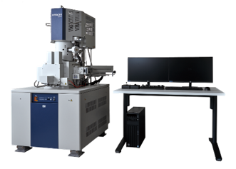
Ultrahigh-Resolution Schottky Scanning Electron Microscope SU8700
The SU8700 brings in a new era of Ultrahigh-Resolution Schottky field emission scanning electron microscopes to the long-standing Hitachi EM line-up. This revolutionary FE-SEM platform incorporates multifaceted imaging, high-probe current, automation, efficient workflows for users of all experience levels, and more.
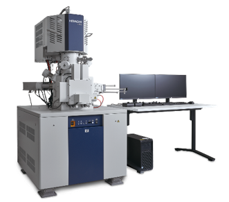
Ultrahigh-Resolution Scanning Electron Microscope SU8600
The SU8600 brings in a new era of Ultrahigh-Resolution cold-field emission scanning electron microscopes to the long-standing Hitachi EM line-up. This revolutionary CFE-SEM platform incorporates multifaceted imaging, automation, increased system stability, efficient workflows for users of all experience levels, and more.
Ultrahigh-Resolution Schottky Scanning Electron Microscope SU7000
The SU7000 is designed to allow simultaneous acquisition of multiple secondary and backscattered electron signals, and enables rapid capture of many types of signals. With the ability to display and store up to 6 signal channels simultaneously, the SU7000 offers unsurpassed imaging performance. In addition, it provides a flexible of specimen chamber and vacuum system to support the broad range of observational conditions. Moreover, the electron gun—with its built-in Schottky emitter—can provide irradiating beam currents of up to 200 nA. The SU7000 is built to accommodate the full diversification of future analytical methods.
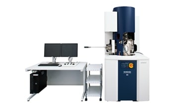
Schottky Field Emission Scanning Electron Microscope SU5000
SU5000 combines Schottky emission electron source and out-lens objective lens for high resolution imaging and diverse analyses of samples with various sizes and compositions. Its drawer type stage allows applications with special stages such as heating, tensile, and so on. Unique user interface, EM Wizard supports best SEM experience of every user.
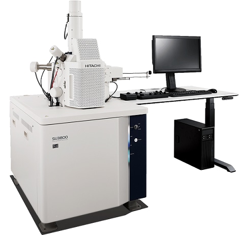
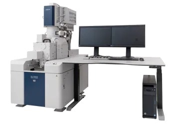
Scanning Electron Microscopes SU3800/SU3900
Hitachi High-Tech's scanning electron microscopes SU3800/SU3900 deliver both operability and expandability. The operator can automate many operations and efficiently utilize their high performance. The SU3900 is equipped with a large multipurpose specimen chamber to accommodate observation of large samples.
Scanning Electron Microscope FlexSEM 1000 / FlexSEM 1000 II
FlexSEM 1000 employs thermionic electron source and achieves resolution of 4.0nm with its compact design ready for desktop setup. Low vacuum mode allows rapid observation of insufficiently conductive samples without metal coating to prevent charging. Optional Ultra Variable pressure Detector (UVD) enhance surface imaging capability of samples under low vacuum environment.
Field Emission Transmission Electron Microscope HF5000
Hitachi's unique 200 kV aberration-corrected TEM/STEM: the perfect harmony of imaging resolution and analytical performance
0.078 nm spatial resolution in STEM is achieved together with high specimen-tilt capability and large solid angle EDX detector(s), all in a single objective lens configuration.
The HF5000 builds on features from Hitachi HD-2700 dedicated STEM including Hitachi's own fully automated aberration corrector, symmetrical dual SDD EDX and Cs-corrected SE imaging. It also incorporates the advanced TEM/STEM technologies developed in the HF series.
Integrating these accumulated technologies into a new 200 kV TEM/STEM platform results in an instrument with an optimum combination of sub-Å imaging and analysis, as well as the flexibility and unique capabilities to address the most advanced studies.
Transmission Electron Microscope HT7800 Series
The HT7800 series is a 120 kV transmission electron microscope (TEM) that combines high-quality and reproducible data acquisition with improved efficiency for observation work.
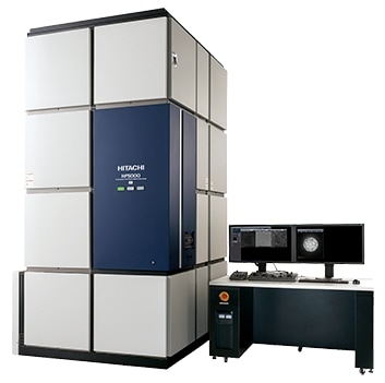
Real-time 3D analytical FIB-SEM NX9000
SEM column and FIB column are orthogonally arranged to optimize column layout for 3D structural analysis. FE electron source and its unique detection geometry enable high resolution SEM imaging at beam coincident point. 3D-EDS and 3D-EBSD can be performed without moving the stage. Employing micro-sampling and triple beam system, high quality samples can be prepared for TEM and atom probe.
Focused Ion and Electron Beam System
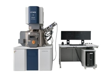
Ethos NX5000
The Hitachi Ethos FIB-SEM incorporates the latest-generation FE-SEM with superb beam brightness and stability. Ethos delivers high-resolution imaging at low voltages combined with ion optics for nanoscale precision processing.
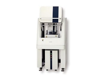
Atomic Force Microscope AFM5500MⅡ
The AFM5500MⅡ is an AFM platform equipped with a fully addressable 4-inch stage, optimized for medium-sized samples.
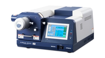
Ion Milling System ArBlade 5000
ArBlade 5000 supports both cross-section milling and flat milling to prepare samples depending on the purpose. Cross section width can be expanded to 8mm for applications requiring wide area milling such as electric components.