
Our group company, VLC Photonics, will issue the white paper “Miniaturize your optical system into a photonic integrated circuit”.
We will distribute the contents of this white paper with this newsletter over 3 weeks.
This time, please let us deliver vol.2 of this whitepaper which include the main technology of Photonic Integration and how Photonic Integration can be done.
Also we will explain the strength of ASPIC compared with other technologies.
White paper includes the market, technology and challenges of Photonic Integrated Circuit,
so we hope you have interest in Photonic Integration and VLC Photonics.
VLC Photonics Whitepaper v2.2 June, 2021
Miniaturize your optical system into a photonic integrated circuit vol.2
Learn how you can benefit from this technology
Summary
Photonic technologies use the light to enable multiple applications nowadays, from optical telecommunications to biomedical diagnostic devices or precise fiber sensors for all kinds of structures.
Still, optical components tend to be bulky and expensive, and require precise stabilization and assembly, especially when interfacing with electronics. Embedding some photonic functionalities into an integrated optical chip can simplify a system and dramatically decrease its costs.
However, the cutting-edge optical manufacturing technologies enabling such chip integration were traditionally affordable only by very few.
Nowadays, generic photonic integration has been demonstrated as a very interesting technology that provides cost effective and high-performance miniaturization for a wide range of applications and markets.
In last issue, Foreground, Background of Photonic integration technologies were reviewed.
And in this issue, we highlight the Main technology and how photonic integration can be done with some characteristics of base material.
Also from the comparison of ASPIC vs micro optics assembly and generic integration, we introduce what is the strength of ASPIC.
Main Integration Technologies
Overview
Different technologies can be chosen to design and manufacture ASPICs, depending on the suitability of the base material to the application at hand.
The most relevant technologies are:
- Silicon photonics : Silicon on Insulator*1(220 nm and 3 μm SOI), and Si based Silica on Silicon*2(SiO2, also known as PLC) and Silicon Nitride*3(SiN and TriPleX)
- III-V photonics : Indium Phosphide*4(InP), Gallium Arsenide (GaAs) and derivatives.
- Lithium Niobate*5(LiNbO3) and other more exotic materials.
Characteristics
Each of these materials has its own strengths and limitations, with their main properties highlighted in the following table:
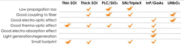
These features will determine which kind of optical components can be implemented in a practical way and deliver the best performance.
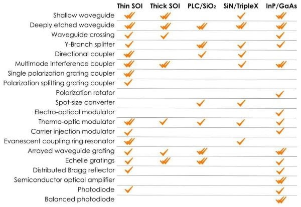
The most common functional components available for each technology, along with their most appropriate material matches, are identified below:
How is integration being done?
Monolithic integration vs. Micro-optic assemblies
The technologies described before are used to fabricate complete optical devices using only a single material chip: this is known as monolithic integration. This goes one step further than the current assembly of micro-optical components in miniature photonic systems.
By integrating all devices into a single substrate, complex assembly, alignment and stabilization processes are avoided, and packaging and testing are greatly simplified.
Moreover, it is the only way to scale system complexity when surpassing more than 20-30 optical components into a single package.
The election of the integration material will then determine the capabilities and design rules for the technology platform, making some of them more appropriate for certain applications than others.
This is thus a critical step into the integration process and needs to be carefully evaluated*6-7.
Specialized vs. Generic integration
ASPIC production has been implemented for years using a model known as specialized integration, which focuses on single devices rather than a complete optical system. This model is based on a prior identification of specific needs for a certain device and a massive market, like in the case of telecom lasers, photo-diodes or power splitters.
To produce this very particular device, a manufacturing facility is set up and a fabrication process is tailored to its development, resulting thus in the best possible performance.
This model is only profitable as long as large series of devices - typically hundreds of thousands - are successfully marketed, due to the huge investment required to deploy and operate such a specialized manufacturing process.
On the other hand, generic integration focuses on applications rather than devices.
Compared to a specialized manufacturing process developed only for a single device, a generic fabrication process makes use of multiple building blocks pre-developed for a generalized manufacturing process.
The combination of these can result in several devices enabling very different solutions and markets.
Under this model, the number of components to be manufactured does not necessarily need to be huge -starting from tens to hundreds of units - as the fabrication process and costs can be shared among many users.
Additionally, if required, a generic fabrication process can also be scaled up to transfer production to larger volumes.
Therefore, the generic integration model allows a low investment access to custom ASPICs, and opens the door for exploring the integrated optics field without a huge investment in R&D.
Reference
- *1
- W. Bogaerts et Al., "Silicon nanophotonic waveguides and their applications,” Proc. SPIE 7134, Nov 2008.
- *2
- C.R. Doerr and K. Okamoto, "Advances in Silica Planar Lightwave Circuits," in Journal of Lightwave Technology, Vol. 24(12), pp. 4763-4789, December, 2006.
- *3
- F. Morichetti et Al., "Box-Shaped Dielectric Waveguides: A New Concept in Integrated Optics?," in Journal of Lightwave Technology, Vol. 25(9), pp. 2579-2589, September, 2007.
- *4
- R. Nagarajan et Al., "InP Photonic Integrated Circuits," IEEE Journal of selected topics in quantum electronics, Vol. 16(5), Sept 2010.
- *5
- W. Sohler et Al., "Integrated Optical Devices in Lithium Niobate," in Optics & Photonics News, Vol. 19(1), pp. 24-31, 2008.
- *6
- D. Liang and J.E. Bowers, "Photonic integration: Si or InP substrates?," in Electronics Letters, Vol. 45(12), pp. 578-581, June, 2009.
- *7
- G.A. Vawter, "Defining capabilities of Si and InP photonics," Proc. of IEEE AVFOP conference, 2010.
Legal Disclaimer
This white paper, © by VLC Photonics S.L. intends to facilitate the knowledge of the trademark, its activities and services. Consequently, VLC Photonics S.L. reserve all rights, especially the rights of reproduction, distribution, communication to the public and transformation.
VLC Photonics S.L. is not responsible for any consequences or damages that may arrive from the use of any of the information contained within this document or its references.
The conditions for the partial reproduction of elements in this white paper are:
- That VLC Photonics S.L. is cited specifically as the source of the information or material.
- That the information and content is cited solely on the basis that it is used for information purposes only and not for commercial gain or any other distinct use that is not private or individual.
- That no content contained in this white paper is modified in whatever form.
- That no image available on this white paper shall be used, copied or distributed separately from the accompanying text or other content that accompanies it.
- That it is communicated in writing and in an irrefutable manner to VLC Photonics S.L. and, that certified authorization is obtained from the company for the stated reproduction.
In next issue, “Main integration technologies” and “how integrations can be achieved” will be explained. Click here to know more about Photonic Integration and VLC Photonics.