
Hitachi High-Tech in Canada
  1. Home
  2. Products & Services
  3. Materials & Components
  4. Electronic Components
  5. Optical communication components
  6. VLC Photonics S.L.

Company Profile

Company Name VLC Photonics S.L.
Location Building 9B (East entrance),
Office 0.71 Universidad Politecnica de Valencia (access I) Camino de Vera s/n – 46022,
Valencia – Spain
Established October, 2011
under Hitachi Group company since Oct.2020
Capital € 112,250
Net Sales Not available
Number of Employees 19 (as of Jul.2022)

VLC Photonics S.L.
Official Website

--

Main Services

  • Photonic Integration Consultancy
  • PIC Design
  • PIC Characterization and Test
  • PIC Packaging
  • PIC Manufacturing
  • Foundry Process Design Kits
  • PIC Design and Characterization trainings

-

Services

-

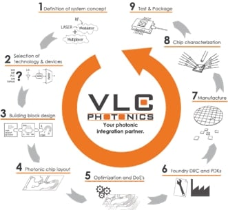
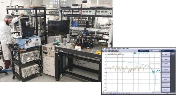
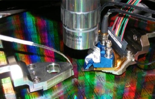
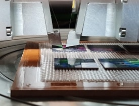
VLC Photonics offers Photonics Integrated Circuit(PIC) development service.

With extensive industrial and academic experience, from different fields like:

  • Telecom/Datacom
  • Sensing
  • Quantum
  • Metrology
  • LIDAR
  • Bio Photonics

VLC Photonics is a fabless company offering different solutions exploiting the advantages of PIC.

We are able to provide either turn-key solutions making use of photonic integration or specific services along the whole development process depending on customer needs.

With the wide network of Hitachi group, VLC Photonics offers the solution from prototype to volume production.

-
-
--

(New) Wafer Level Testing with edge coupling

Wafer Level Testing with edge coupling

Capabilities

  • Automated wafer level testing tool in clean-room environment
  • System adopted for Edge Coupling via on-wafer structures
  • Use of optical coupling system with fibers and fiber arrays
  • 2 optical probes, allowing for single fiber or fiber arrays
    (no hard limit in terms of fiber array size or SMF vs. PMF)
  • Up to 2 electrical DC probes and 2 electrical RF probes*
    *160 & 250 um pitch, GS/GSG/coplanar configuration
  • Thermally controlled chuck for single dies and wafers of 3'' to 12”
-

(New) High-Speed RF Characterization

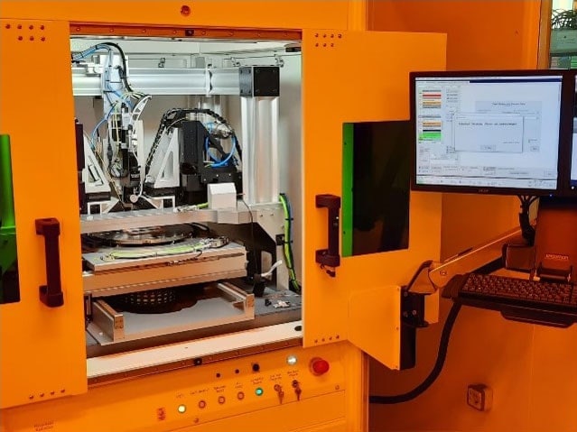
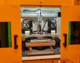
To be installed new equipment

High-Speed RF Characterization

Capabilities

  • N4372E Lightwave Component Analyzer is available at VLC Photonics
  • Opto-Electric S-parameter measurement up to 110GHz
  • Traceable S21 measurement across the entire CWDM wavelength range,1260nm to 1620nm
  • Available for E/O, O/E, O/O, E/E Test
  • Measurement Capabilities
    Responsivity (S21, amplitude and phase), Reflectivity (S11, S22 amplitude and phase)
  • Adoptable to Wafer Level Testing (Under development)

Find More Products

(New!) Wafer Level Testing

- - -

- -

Capabilities

  • fully automated wafer level testing tool in clean-room environment
  • 6 degrees of freedom for each probing arm
  • two optical probes, allowing for single fiber or fiber arrays
    (no hard limit here in terms of fiber array size or SMF vs. PMF)
  • up to two electrical DC probes (standard pitches)
  • up to two electrical RF probes
    (160 & 250 um pitch, GS/GSG/coplanar configuration, up to 40 GHz)
  • thermally controlled chuck for single dies and wafers of 3'' to 12‘’

-

Find More Products

Back to Top