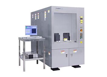
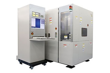
Defect and Pattern Evaluation SEM CT1000
3D observation capability contributing
“to Shorten development cycle“ and
“to enhance product quality“ of G&C device*1
Once a wafer of up to 200 mm in size has been transported automatically, CT1000 moves precisely to the critical pattern position, or the defect position detected by the defect inspection unit. Three-dimensional SEM observation can then be performed using a tilting sample stage. CT1000 also has an energy-dispersive X-ray spectrometer (EDS) *2 that can be used to infer the elements contained in the sample for observation.
*1)
G&C device is an abbreviation for Green & Communication Device.
Specifically, electronic devices and electronic components manufactured
on φ100/125/150/200mm wafers.
(Ex: SAW / BAW, MEMS and sensors, power and analog devices, etc.)
*2) Option
* Signal tower: Option
Features
- 5-axis specimen stage enabling 3D observation of defect and pattern shape
- Integrating EDS* enabling to identify element of defect (EDS: Energy dispersive X-ray analysis system)
- Support φ100 mm, φ150 mm, φ200 mm wafer
* Option
Specifications
| Resolution | 7 nm@1 kV |
|---|---|
| Maximum sample tilt angle | 55° |
| Size of observation field | 0.675~135 µm |
| Elemental analysis (option) | Energy-dispersive X-ray spectrometer |