
Hitachi High-Tech in Europe
  1. Home
  2. Products & Services
  3. Electron Microscopes / Atomic Force Microscopes
  4. Focused Ion Beam Systems (FIB/FIB-SEM)

Focused Ion Beam Systems (FIB/FIB-SEM)

Focused Ion Beam System (FIB/FIB-SEM) Lineup

-

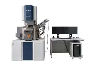
Focused Ion and Electron Beam System Ethos NX5000

The Hitachi Ethos FIB-SEM incorporates the latest-generation FE-SEM with superb beam brightness and stability. Ethos delivers high-resolution imaging at low voltages combined with ion optics for nanoscale precision processing.

-

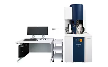
Real-time 3D analytical FIB-SEM NX9000

SEM column and FIB column are orthogonally arranged to optimize column layout for 3D structural analysis. FE electron source and its unique detection geometry enable high resolution SEM imaging at beam coincident point. 3D-EDS and 3D-EBSD can be performed without moving the stage. Employing micro-sampling and triple beam system, high quality samples can be prepared for TEM and atom probe.

-

Focused Ion and Electron Beam System & Triple Beam System NX2000

NX2000 was developed towards the ultimate TEM sample preparation system. FE electron source and high-sensitivity detection system allow high-contrast, real-time end point detection. Sample orientation control technology and Ar/Xe triple beam system enable significant reduction of artefacts and damage during sample preparation. With auto micro-sampling function, the throughput of TEM sample preparation can be drastically improved.

-

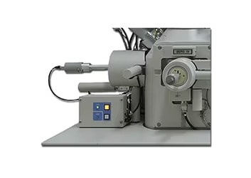
Micro-sampling System

This device is used for preparing the desired wafer part for analysis with STEM, TEM, etc. by extracting a micro sample with an ion beam in the vacuum chamber of an FIB system.

-

CAD Navigation System NASFA (Navigation System for Failure Analysis)

The CAD Navigation System for Failure Analysis (NASFA) is used to identify the location on the CAD data corresponding to the LSI pattern being observed with a SEM or FIB system. When the coordinates on the CAD data are specified, the sample stage moves to the particular coordinates, displaying the corresponding SEM image (or SIM image for the FIB). The CAD data and SEM image can be overlaid and it is easy to verify the lower-layer wiring location, significantly improving the efficiency of analysis and repair work.

Related Information